In a wireless communication terminal, the low noise amplifier (LNA) serves as the first active stage in the radio frequency (RF) receiving system. Its primary role is to amplify the weak signal received by the antenna from the air while minimizing noise interference, ensuring that the system can accurately demodulate the desired information. The design of the LNA plays a crucial role in determining the overall performance of the receiver. A well-designed LNA should provide maximum gain without distortion, maintain good linearity, and minimize noise contribution to the signal. To address noise issues effectively, a common-base differential input structure was proposed for the LNA circuit design. This configuration helps reduce noise while maintaining high gain. The circuit includes a controllable gain amplifier along with a gain control circuit, allowing for dynamic adjustment based on signal strength. The output voltage of the LNA is directly connected to the automatic gain control (AGC) circuit. Depending on the level of this output, the AGC adjusts its own output, which is then fed back into the comparator of the gain control circuit. This feedback mechanism allows the LNA to maintain an optimal gain level under varying input conditions. The amplifier was designed using the Jazz 0.35 μm BICMOS process, ensuring low noise and high gain performance. 1. Noise Problems in Low Noise Amplifier Design One of the most common sources of noise in electronic circuits is flat-band noise, also known as white noise. This type of noise arises from both shot noise and thermal noise. Shot noise occurs due to the quantum nature of electrons crossing a barrier, typically found in diodes and bipolar transistors. It requires two conditions: the presence of a DC current and the movement of charge carriers across the barrier. The shot noise current can be calculated using the formula: I_n = √(2qI_DΔf), where q is the elementary charge, I_D is the junction current, and Δf is the noise bandwidth. As shown, shot noise is proportional to the square root of the junction current and is independent of frequency and temperature. When multiplied by the dynamic junction impedance, it can be expressed as a noise voltage. Thermal noise, on the other hand, results from the random motion of charge carriers within a device. Any component with a DC resistance will generate thermal noise. Since this noise is random and follows a Gaussian distribution, it is usually characterized by measuring the average noise power. The thermal noise power is given by: P_n = 4kTΔf, where k is the Boltzmann constant (1.38 × 10â»Â²Â³ J/K), T is the absolute temperature, and Δf is the noise bandwidth. The thermal voltage produced by a resistor at a given temperature and bandwidth is expressed as: V_n = √(4kTRΔf), where R is the resistance value. By dividing both sides of this equation by R, we obtain the Norton equivalent noise source. Normalizing the RMS noise voltage and current to a 1 Hz bandwidth gives the noise spectral density. This helps in understanding how noise behaves across different frequencies. If the signal amplitude increases faster than the noise, improving the circuit’s performance becomes possible by increasing the noise level. This principle is often used in optimizing the signal-to-noise ratio in various applications. 2. Low Noise Amplifier Design 2.1 Structural Design of Low Noise Amplifier Circuit Two common types of LNAs are those with bipolar and CMOS inputs. While CMOS amplifiers are known for their low input bias currents, they tend to have higher voltage noise. A typical CMOS amplifier may exhibit flat-band noise in the tens of nV/Hz range, with 1/f noise reaching a few microvolts peak-to-peak. Bipolar amplifiers, however, are generally preferred for low-noise applications due to their lower noise levels. In RF applications, the main noise sources in MOSFETs include channel thermal noise, gate-induced noise, and gate distributed resistance noise. Due to the relatively high thermal noise from the channel resistance, using a bipolar input often leads to a better noise figure. Low-noise bipolar amplifiers offer extremely low input voltage noise density and relatively higher input current noise density. Single-ended LNA structures are highly sensitive to ground parasitic inductance. In contrast, differential structures use AC grounding at the symmetry point, making them less affected by parasitic parameters in the current source loop. Additionally, differential amplifiers excel at rejecting common-mode interference, which is especially important in mixed-signal systems where supply and substrate voltages may contain noise. To maximize the common-mode rejection ratio at high frequencies, layout symmetry is essential. Differential structures also contribute significantly to noise suppression. The common base configuration in bipolar LNAs offers advantages such as simpler input matching, better linearity, and improved reverse isolation, which makes it a preferred choice in many designs. 2.2 Circuit Design of Low Noise Amplifier The overall structure of the LNA is illustrated in Figure 1. The circuit is divided into three main modules. The VGLNA module is a controllable gain amplifier, capable of adjusting its gain dynamically. The CON1 and CON2 modules are gain control circuits that regulate the gain of the VGLNA using the AGC control voltage. The design goal for VGLNA is to achieve a minimum gain of 25 dB. Meanwhile, the CON1 and CON2 modules are designed to ensure that the VGLNA's gain remains within the AGC’s dynamic range by adjusting the voltage levels at nodes IN1 and IN2. Carbon Fiber FPV Drone Frame,FPV Drone TrueX Frame,Carbon Fiber FPV Frame Jiangsu Yunbo Intelligent Technology Co., Ltd , https://www.fmodel-ai.com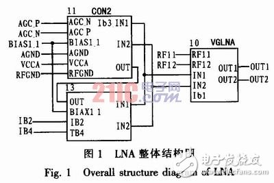
Mark4 V2 Mark4 7inch 295mm / 8inch 367mm / 9inch 387mm / 10inch 427mm 3K Full Carbon Fiber TrueX Frame for FPV Camera Kit Done:


Low Noise Amplifier Design Based on JAZZ 0.35 μm BICMOS Process
FPV Drone TrueX Frame Overview