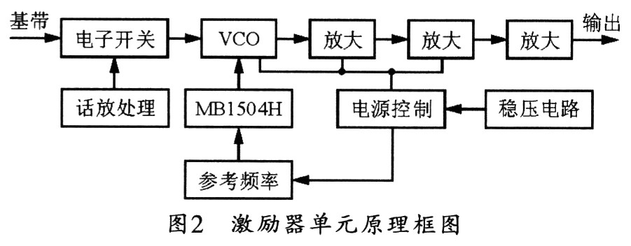
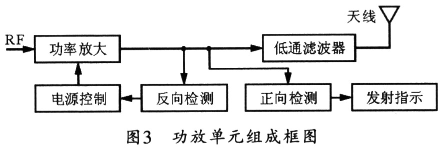
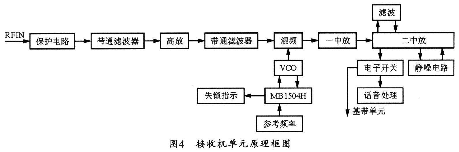
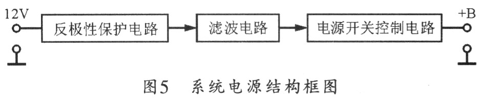
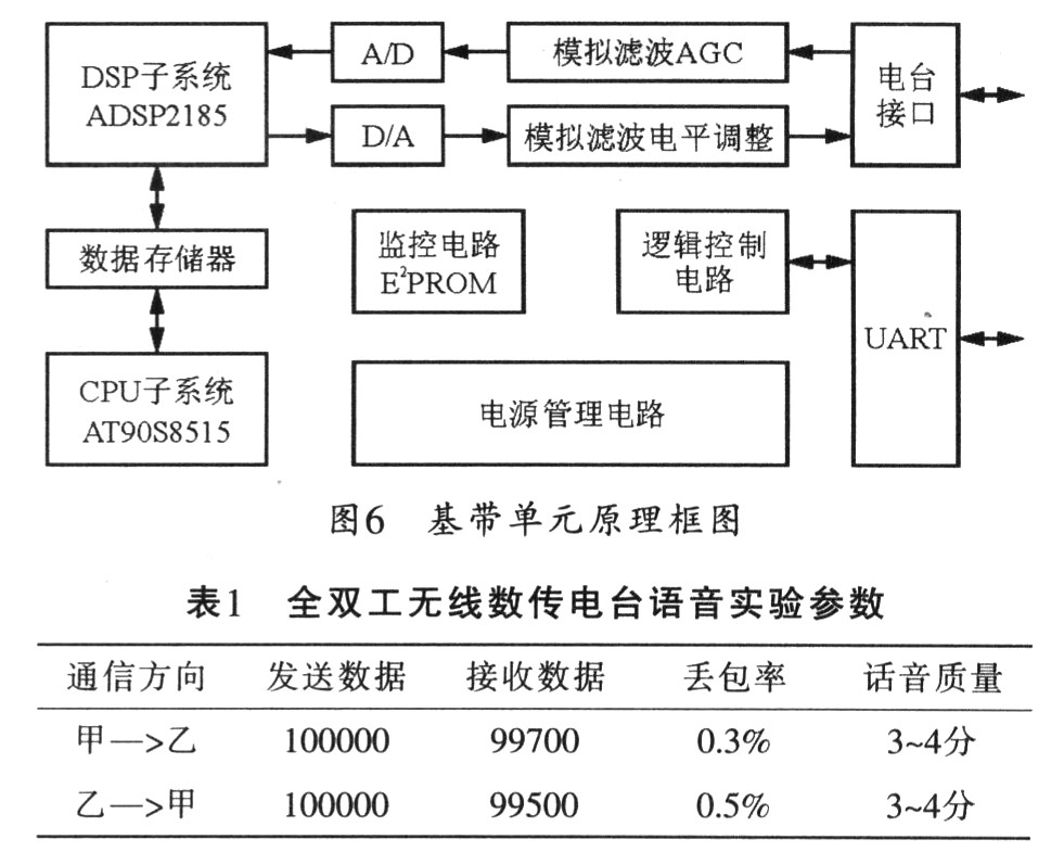
Design scheme of full-duplex wireless digital radio station 0 Preface The application of digital radio in the field of industrial control has been very extensive, and it is still the main transmission method in the field of industrial control. As a simplest communication method, the wireless digital radio station has the most basic features of convenient and simple communication. However, at present, the vast majority of domestic and foreign are simplex radio stations. Full-duplex digital radio stations are still rare, and some engineering projects do require full-duplex digital radio stations for data transmission. Therefore, this paper proposes a design concept for full-duplex digital radio stations. 1 The structural principle of a full-duplex wireless digital radio station The full-duplex digital radio station introduced in this article mainly uses the frequency division duplex (FDD—Frequency Division Duplexing) working mode. It is mainly composed of six parts: receiving unit, exciter unit, power amplifier unit, control unit, power supply unit, and baseband unit. Figure 1 shows the block diagram of its structure. 2 System structural unit design 2.1 Exciter unit The exciter unit completes the modulation of the radio frequency signal and the processing of the audio signal, that is, the voice and data to be modulated are sent to the VC0 modulation and the voltage is amplified. It consists of speech amplifier processing, digital phase-locked loop, voltage controlled oscillator, voltage amplifier, power adjustment circuit, and power supply circuit. Figure 2 shows the block diagram of the exciter unit. In the picture, the weak signal sent by the microphone is first sent to the voice amplifier processing circuit for signal processing such as voice amplification, filtering, pre-emphasis, and then sent to the voltage-controlled oscillator through the electronic switch for direct frequency modulation. The digital signal is also sent to the voltage controlled oscillator for direct frequency modulation after being switched by the electronic switch. A fast recovery diode can be used for the phase-locked loop to improve the locking speed of the phase-locked loop, a passive proportional integral filter can be used for the loop filter, and a modular design is used for the VCO. The digital phase-locked loop chip adopts MBl504H integrated circuit chip of Fujitsu of Japan. The chip has a high degree of integration and small size, especially its pump power supply is up to 8 V, which can relatively reduce the VCO voltage control sensitivity. In order to reduce the frequency variation of the transmitter in a wide temperature range, it is recommended to use a temperature compensated crystal oscillator as the reference frequency. Because the signal output by the VCO is weak, only a few milliwatts, it can be sent to the phase discriminator to be compared with the reference frequency after passing through the power divider, and an error voltage is generated to control the frequency of the VCO to the set frequency point. The other way is sent to the voltage amplifier, and then subjected to 3-level amplification processing, so that it can promote the work of the power amplifier circuit. Considering the general need to connect an external battery as a power source, the power input of the exciter can be stabilized with a 7809 three-terminal regulator to provide a wider voltage dynamic range. At the same time, multi-level LC filtering can also be used to improve voltage regulation and noise reduction. 2. 2 power amplifier unit The main task of the power amplifier unit is to amplify the RF signal sent by the exciter to 44 dBm through the power amplifier module, then pass the low-pass filter to filter out the higher harmonics, and then send it to the duplexer, and finally transmit it through the antenna. If the antenna is open or shorted, the power will be reflected back. At this time, the detection circuit will detect and then amplify, and then send a signal to the MCU. The MCU controls the relevant circuit to turn off the power amplifier to achieve the purpose of protecting the power amplifier module. The composition of the power amplifier circuit is shown in Figure 3. 2. 3 receiver unit The receiving unit can complete the demodulation of the radio frequency signal and the processing of the audio signal. It is generally composed of filter, selective loop, high amplifier, double balanced mixer, first middle amplifier, second middle amplifier. Among them, the second intermediate amplifier is composed of two local oscillators, two frequency mixers, phase discriminator, and noise control circuit. The first intermediate frequency in the mixer is 21.4 MHz, the second intermediate frequency is 455 kHz, and the mixing method is heterodyne. When the radio frequency signal is sent to the duplexer through the antenna, it is filtered by the first-stage band-pass filter, and then sent to the high-amplifier circuit after limiting. Then enter the second-stage band-pass filter for filtering, and finally send it to the double-balanced mixer for mixing. The function of the limiting circuit is to prevent the strong interference signal from damaging the high-end front-end components. The high-amplifier circuit generally adopts a double-tuned loop and a first-stage amplification form, and the input and output loops use a tap form to make the circuit match and gain. The high-discharge tube can choose the low-noise tube 2SC3356, which is characterized by low noise and high power gain. The signal amplified by the high amplifier is mixed with the first local oscillator signal sent by the voltage control through a double-balanced mixer. 2SC3356 is an integrated component, characterized by low noise and few high-order combinations. A signal with an intermediate frequency of 21.4 MHz can be sent to the intermediate amplifier integrated circuit TA31136FN after two stages of intermediate frequency amplification, and mixed with the second local oscillator generated by the 20.945 MHz crystal oscillator, and the mixed 455 kHz second intermediate frequency signal, After filtering through a 455 kHz ceramic filter, it passes through the 5-pin input of the second amplifier. The output of the limiting amplifier can be directly driven internally, and the frequency discrimination can be completed externally through the phase shift coil. The audio signal output by the frequency discrimination is output by pin 9. The signal is sent all the way through the electronic switch to de-emphasis, filtering, and amplification to the speaker to restore the sound. The other way is sent to the baseband signal processor after filtering. The digital phase-locked loop in the receiver can be designed with MBl504 integrated circuit of Fujitsu Corporation of Japan. Due to the high degree of integration and small size of the device, serial data reception programming is simple. Therefore, the RF signal sent by the VCO and the temperature-compensated crystal oscillator is coupled to MBl504H, and then the internal part frequency ratio is compared to obtain the error voltage, and then fed back to the VCO control to fine-tune its frequency, which can be locked on the set channel. When the VCO loses lock, a lock-out indication circuit can also provide a lock-out level to light up a SMD LED, which provides convenience for subsequent maintenance. Figure 4 is a block diagram of the principle structure of the receiver unit. 2.4 Power supply design Through the system power supply, the external DC power supply can be filtered, reverse polarity protection, etc., and then a stable power supply voltage is output. At the same time, the power supply must also perform the necessary short circuit and overcurrent protection. The system power supply can be connected to +12 V DC, and then reverse polarity protection circuit to prevent the power supply from being reversed. After passing through a multi-level LC filter circuit to filter out various clutter and high and low frequency AC interference, it is sent to the power supply relay, and the relay control panel power switch is used to switch the power supply of the whole machine. The structure schematic diagram of its power circuit is shown in Figure 5. 2.5 Control and baseband unit The control unit uses ATMEGA64 as the core to complete the control of the working state of the machine, including the frequency combination data of the transceiver, the control of the panel display and the keyboard, the control of the working frequency band, the data transmission and the control of the voice communication state. The baseband unit handles the data exchange between the machine and the computer terminal. It takes DSP chip ADSP-2185M as the core, and uses microcontroller AT90S8515 and CPLD complex programmable logic device to form the control and interface circuit. At the same time, the interface circuit of the signal and the radio station is formed by digital-to-analog and analog-to-digital conversion, and an operational amplifier. The baseband unit uses DSP to modulate and demodulate digital signals. Figure 6 shows the principle block diagram of the baseband unit. 3 Whole machine communication test After the prototype is designed, it can be tested. During the test, the height of the antenna should be 6m, the omnidirectional antenna can choose a high gain antenna of 7.8dBi, and the linear distance between the two devices should be greater than 30km. After setting, you can send and receive data through the serial debugging assistant and perform full-duplex data communication. The channel rate can be selected as 19200 bps, each packet is 100 bytes, and the PTT delay is selected as 20 ms. In general, the system voice quality and packet loss rate should meet the parameters listed in Table 1. 4 Conclusion This paper presents a design scheme of a full-duplex wireless data transmission station. The full-duplex wireless data transmission station designed by this scheme has good stability, high reliability, good high and low temperature characteristics, and low failure rate. As long as the selection of electronic components in the system is correct, generally a certain stability can be achieved, and the reliability is also very good. Optical Distribution Frame is applicable for flexible cabling access, expandable frame design and comprehensive cable management,which can be conveniently pulled out like a drawer.With standard 19" size,Fiber Distribution Frame is made of cold-rolled sheet and comes with a metal front door. Its drawer guide rails allows fiber optic ODF to be pulled out effortlessly. The optical fiber distribution frame can be installed on the existing wiring rack.A series of ODF optical distribution frame is 12 fibers ODF, 24 fibers ODF, 48 fibers ODF, 72 fibers ODF,96 fibers ODF and 144 fibers ODF counts type.All are withdrawable and widely utilized for wiring and connection between fiber optic cables and FTTH projects. Optical Distribution Frame Optical Distribution Frame,ODF Fiber,Fiber Distribution Frame,ODF Fiber Optic Foclink Co., Ltd , https://www.scfiberpigtail.com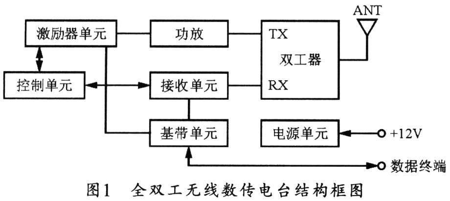
Foclink,a reliable supplier of optical distribution frame,is always beside u 7*24.