There is a CPU inside the 51 MCU for operation and control. There are four parallel I/O ports, which are P0, P1, P2, P3, and have ROM for storing programs. There is RAM for storing intermediate results. There are also timer/counters, serial I/O ports, interrupt systems, and an internal clock circuit. There are separate memory locations in the microcontroller that are used to control these devices and are referred to as Special Function Registers (SFRs). There are a total of 21 such special function registers 51, and all of them are addressable as follows (the special function registers added to the 52 series with *): Shenzhen Kaixuanye Technology Co., Ltd. , https://www.iconlinekxys.com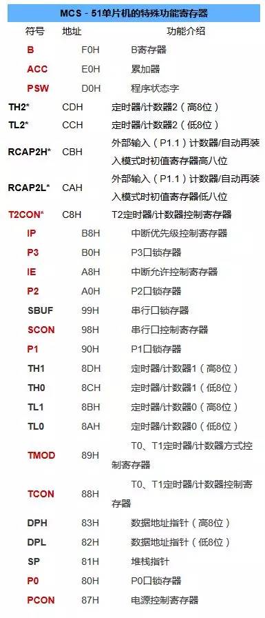 The explanations are as follows: 1. ACC--- is an accumulator. Usually, A is used to indicate what this is. It can't be understood from the name. It is a register, not a thing to do addition. Why give it a name? Perhaps it is because one of the numbers in the operator must be in the ACC. Its name is special and its identity is special. We will learn the instructions later in the middle part, and we can find that all the arithmetic instructions are inseparable from it. It has its own zero mark Z, Z = 1 if A = 0, and z = 0 if A ≠0. This flag is often used as a condition for the branching of program branches. 2, B - a register in the multiplication, division, multiplier or divisor, do not do multiplication and division, how to use it. 3, PSW-----program status word. This is a very important thing, which puts a lot of state when the CPU works, so that we can understand the current state of the CPU and handle it accordingly. Please see the table below for its features:
 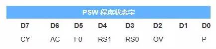 Below we introduce each person's use CY: carry flag. The 8051 operator is an 8-bit arithmetic unit. We know that the 8-bit operator can only represent 0-255. If adding, the two numbers may add more than 255, so the highest bit will be lost. What should I do if I make a mistake in the operation? The highest position comes here. This will be fine. There are advances, borrows, CY=1; no advance, borrow, CY=0 : 78H+97H (01111000+10010111) AC: auxiliary advance, borrow (between high nibble and low nibble, excuse me). Example: 57H+3AH (01010111+00111010) F0: The user flag is determined by the user (programmer) when and when. RS1, RS0: Working Register Group Select Bits You can select a working register area by modifying the state of RS1 and RS0 in the PSW. This feature increases the speed of the MCS-51 field protection and on-site recovery. It is advantageous to increase the efficiency of the CPU and the speed of response interruption. If in a real application system, four sets of working registers are not needed, then the extra units in this area can be used as general data buffers.
 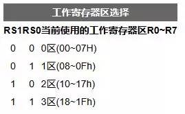 0V: The overflow flag bit operation result is understood by the complement code operation. There is overflow, OV=1; no overflow, OV=0. What is overflowing will be covered in the chapters that follow us. P: Parity bit It is used to indicate the parity of the number of binary digits "1" in the ALU operation result. If it is an odd number, P=1, otherwise it is 0. The result of the operation has an odd number of 1, P = 1; the result of the operation has an even number of 1, P = 0. Example: The result of a certain operation is 78H (01111000). Obviously, the number of 1 is even, so P=0. 4, DPTR (DPH, DPL) -------- Data pointer can be used to access any unit in the external data memory, if not used, can also be used as a general purpose register, we decide how to use. Divided into two registers, DPL (lower 8 bits) and DPH (higher 8 bits). It is used to store 16-bit address values ​​to perform data operations in the 64K byte range for off-chip data RAM or program memory by means of indirect or indexed addressing. 5, P0, P1, P2, P3-------- input and output (I / O) register This we already know, is the register of four parallel input / output (I / O). The content inside it corresponds to the output of the pin. 6, IE-----interrupt enable register can be addressed by bit, address: A8H
 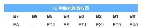 EA (IE.7): When EA=0, all interrupts are disabled (ie no interrupt is generated); when EA=1, the generation of each interrupt is determined by individual enable bits - (IE.6): ET2 is reserved (IE.5) ): Timer 2 overflow interrupt enable (for 8052) ES (IE.4): Serial port interrupt enable (ES=1 enable, ES=0 disable) ET1 (IE.3): Timer 1 interrupt enable EX1 (IE.2) ): External interrupt INT1 interrupt enable ET0 (IE.1): Timer 0 interrupt enable EX0 (IE.0): External interrupt INT0 interrupt enable 7, IP-----Interrupt priority control register can be bitwise addressed , address bit B8H
  - (IP.7): Reserved - (IP.6): Reserved PT2 (IP.5): Timed 2 interrupt priority (for 8052) PS (IP.4): Serial port interrupt priority PT1 (IP.3): Timer 1 interrupt priority PX1 (IP.2): External interrupt INT1 interrupt priority PT0 (IP.1): Timer 0 interrupt priority PX0 (IP.0): External interrupt INT0 interrupt priority 8, TMOD-----timing The device control register is not addressed by bit, address 89H
 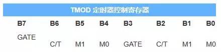 GATE: Timed operation switch control bit. When GATE=1, INT0 or INT1 pin is high level, and when TR0 or TR1 control bit in TCON is 1, the timer/counter 0 or 1 starts to work. If GATE=0, the timer/event 0 or 1 will start to work as long as the TR0 or TR1 control bit is set to 1. C/T: Select bit for the timer or counter function. C/T=1 is the counter, and the count pulse is input through the external pin T0 or T1. When C/T=0, it is a timer, and the timing pulse is provided by the internal system clock. M1, M0: T0, T1 working mode selection bits
 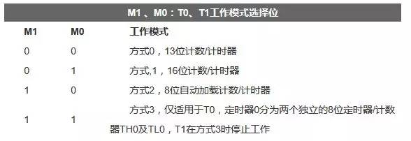 9, TCON-----Timer control register can be addressed by bit, address bit 88H
 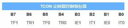 TF1: Timer T1 overflow flag, which can be queried and cleared by the program. TF1 is also the source of the interrupt request. It is cleared by hardware when the CPU responds to the T1 interrupt. TF0: Timer T0 overflow flag, which can be queried and cleared by the program. TF0 is also the source of the interrupt request. It is cleared by hardware when the CPU responds to the T0 interrupt. TR1: T1 is allowed to count the control bit. When it is 1, the T1 count is allowed. TR0: T0 is allowed to count the control bit. When it is 1, the T0 count is allowed. IE1: External interrupt 1 request source (INT1, P3.3) flag. IE1=1, external interrupt 1 is requesting an interrupt from the CPU. When the CPU responds to the interrupt, it clears "0" IE1 (edge ​​trigger mode) by hardware. IT1: External interrupt source 1 trigger mode control bit. IT1=0, the external interrupt 1 program is the level trigger mode, when INT1 (P3.3) input low level, set IE1. IE0: External interrupt 0 request source (INT0, P3.2) flag. IE0=1, external interrupt 1 is requesting an interrupt from the CPU. When the CPU responds to the interrupt, it clears "0" to IE0 (edge ​​trigger mode) by hardware. IT0: External interrupt source 0 trigger mode control bit. IT0 = 0, external interrupt 1 program control is level trigger mode, when INT0 (P3.2) input low level, set IE0. 10. SCON----Serial Communication Control Register It is an addressable special register for serial data communication control. The unit address is 98H. Its structure is as follows:
 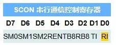 (1) SM0, SM1: Serial port working mode control bits. SM0, SM1 Operation mode 00 Mode 0 - Baud rate is determined by the oscillator frequency: Oscillator frequency / 12 01 Mode 1 - Baud rate is determined by the overflow rate of timer T1 or T2 and SMOD: 2SMOD × (T1 overflow rate) /32 10 Mode 2 - Baud rate is determined by oscillator frequency and SMOD: 2SMOD × Oscillator frequency / 64 11 Mode 3 - Baud rate is determined by the overflow rate of timer T1 or T2 and SMOD: 2SMOD × (T1 overflow rate ) / 32 (2) SM2: Multi-machine communication control bit. <br> Multi-machine communication works in mode 2 and mode 3, and SM2 bit is mainly used in mode 2 and mode 3. Receive status, when the serial port works in mode 2 or 3, and SM2=1, the received first 8 bits of data are sent to SBUF only when the 9th bit data (RB8) is received. Bit RI issues an interrupt request, otherwise the received data will be discarded. When SM2 = 0, regardless of whether the first bit data is 0 or 1, it is rare that data is sent to the SBUF and an interrupt request is issued. When working in mode 0, SM2 must be 0. (3) REN: Allow receiving bits. < br> REN is used to control the permission and prohibition of data reception. When REN=1, it is allowed to receive. When REN=0, it is forbidden to receive. (4) TB8: Transmit received data bit 8. <br> In mode 2 and mode 3, TB8 is to be transmitted - that is, the 9th data bit. This bit is also transmitted in multi-machine communication, and it represents the address or data of the transmission, TB8=0 is the data, and TB8=1 is the address. (5) RB8: Receive data bit 8. In mode 2 and mode 3, RB8 stores the received ninth bit of data for identifying the received data feature. (6) TI: Transmit interrupt flag bit. Addressable flag bit. In mode 0, after the 8th bit of data is transmitted, it is set by hardware. In other modes, it is set by hardware before the transmission or stop bit. Therefore, TI=1 means the frame transmission ends, and TI can be cleared to "0" by software. (7) RI: Receive interrupt flag bit. Addressable flag bit. After receiving the 8th bit of data, this bit is set by hardware. In other modes of operation, this bit is set by hardware, and RI=1 means frame reception is completed. 11. PCON-----The power management register PCON is mainly a special register set for the power control of the CHMOS type MCU. The unit address is 87H, and its structure is as follows:
 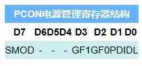 In the CHMOS type MCU, except for the SMOD bit, all other bits are dummy. SMOD is the serial port baud rate multiplication bit. When SMOD=1, the serial port baud rate is doubled. The system reset defaults to SMOD=0. 12, T2CON-----T2 status control register
  TF2: T2 overflow interrupt flag. TF2 must be cleared to "0" by the user program. When T2 is used as the serial port baud rate generator, TF2 will not be set to "1". EXF2: Timer T2 external interrupt flag. When EXEN2 is 1, the interrupt flag DXF2 is set when a negative transition occurs in T2EX (P1.1), and EXF2 must be cleared to "0" by the user program. TCLK: Transmit clock selection flag for the serial interface. When TCLK=1, T2 operates in the baud rate generator mode. RCLK: Receive clock select flag for the serial interface. When RCLK=1, T2 operates in the baud rate generator mode. EXEN2: External interrupt enable flag for T2. C/T2: External counter/timer selection bit. When C/T2=1, T2 is the external event counter, the counting pulse is from T2 (P1.0); when C/T2=0, T2 is the timer, and the dipole signal of the oscillation pulse is used as the counting signal. TR2: T2 count/timing control bit. When TR1 is 1, the count is allowed, and when it is 0, the count is prohibited. CP/RL2: Capture and constant auto-reload mode selection bits. When it is 1 time, it works in the capture mode. When it is 0, T2 works in the constant automatic reload mode. When TCLK or RCLK is 1, CP/RL2 is ignored and T2 always operates in constant auto-reload mode. In the following, the D0, D2, D4, and D5 of T2CON mainly control the working mode of T2. The following summarizes the combination relationship of these bits.