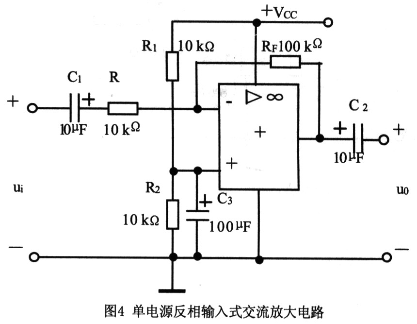
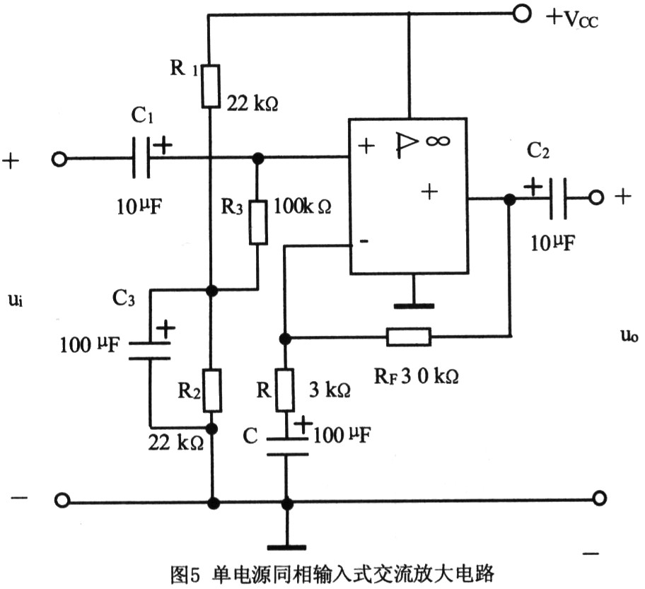
Single-supply op amp AC amplifier circuit In the AC amplifying circuit using capacitive coupling, when the DC voltage at the output of the integrated operational amplifier is not zero, the output voltage of the amplifying circuit is still zero due to the DC blocking effect of the output coupling capacitor. Therefore, the integrated op amp is not required to meet the zero output requirement at zero input. Therefore, the integrated op amp can be powered by a single power supply. The -VEE terminal is connected to the ground (ie, the DC power supply is negative), and the +Vcc terminal of the integrated operational amplifier is connected to the positive pole of the DC power supply. At this time, the voltage V0 at the output of the operational amplifier can only be Change from 0 to +Vcc. In a single-supply operation op amp AC amplifier circuit, in order to prevent distortion of the amplified AC signal, in static state, the voltage V0 of the op amp output terminal is generally set to the middle of the value of 0 to +Vcc, that is, V0=+Vcc /2. In this way, a large dynamic range can be obtained; when dynamic, V0 increases to a value close to +Vcc on the basis of the value of +Vcc/2, and drops to near 0V, and the amplitude of the output voltage uo is approximately Vcc/2. Figure 3, please see the manuscript 1.2.1 Single-supply, non-inverting input AC amplifier circuit Figure 3 is a non-inverting input AC amplifying circuit using a single power supply. The power supply Vcc is divided by R1 and R2, so that the potential of the non-inverting input terminal of the operational amplifier is DC-independent DC, so that RF is introduced into DC full negative feedback. Therefore, the voltage at the output of the op amp is static V0 = V - ≈ V + = + Vcc / 2; C through the AC, so that RF is introduced into the AC part of the negative feedback, is the voltage series negative feedback. The voltage gain of the amplifier circuit is The input resistance of the amplifier circuit is Ri=R1/R2/rif≈R1/R2, The output resistance of the amplifying circuit is R0=r0f≈0. 1.2.2 Single-supply Inverting Input AC Amplifying Circuit Figure 4 is an inverting input AC amplifying circuit using a single power supply. The power supply V cc is divided by R1 and R 2 to make the op amp non-inverting input potential In order to avoid the interference of the ripple voltage of the power supply to the V+ potential, the filter capacitor C3 can be connected in parallel with R2 to eliminate the resonance; since the C1 is separated by DC, the RF is introduced into the DC full negative feedback. Therefore, when static, the voltage at the output of the op amp is V0=V-≈V+=+Vcc/2; C1 is connected to AC, so that RF is introduced into the AC part negative feedback, which is voltage parallel negative feedback. The voltage gain of the amplifier circuit is The input resistance of the amplifying circuit RiR, the output resistance of the amplifying circuit R0 = r0f ≈ 0. 2 Design of the operational amplifier AC amplifier circuit When designing a single-stage op amp AC amplifier circuit, (1) Select an integrated operational amplifier that meets the requirements for use. In the AC amplifying circuit using capacitive coupling, the temperature drift voltage output from the AC amplifying circuit is small due to the DC blocking of the capacitor. Therefore, the requirements for the drift performance of the integrated operational amplifier can be reduced, and the integrated operational amplifier is mainly selected from the aspects of conversion rate, gain bandwidth, and noise. For pulse signals, wideband AC signals, and video signals, an integrated op amp with a high slew rate and a gain bandwidth of at least 10 times the maximum operating frequency should be used. High-speed and low-noise integrated operational amplifiers, such as the dual-amplifier 4558 and NE5532, are often used in audio AC amplifier circuits with high sound quality requirements. (2) Determine whether to use dual power supply or single power supply. When the conditions of use permit, the op amp AC amplifier circuit should use dual power supply mode to increase the linear dynamic range. When the integrated op amp dual power supply is used, the positive and negative supply voltages are generally symmetrical. And the power supply voltage should not exceed the limit of use, power supply filtering is better. In order to eliminate the low frequency self-excitation caused by the internal resistance of the power supply, a capacitor decoupling of 0.01 to 0.1 μF is often added between the positive and negative power supply wirings and the ground. When using a single power supply, the non-inverting input of the op amp is less than the maximum common-mode input voltage of the op amp. (3) Determine if the input signal is an in-phase input or an inverting input. If the input resistance of the amplifier circuit is required to be large, the non-inverting input AC amplifier circuit should be used. Because the increase in the input resistance of the inverting input AC amplifier circuit affects the voltage gain. It can be seen from the calculation formula of FIG. 2 or FIG. 4 that when the input resistance of the inverting input type AC amplifying circuit is increased, the voltage gain of the circuit is reduced, and the voltage gain is also affected by the internal resistance of the signal source. Therefore, when designing an inverting input type AC amplifying circuit, it is sometimes difficult to achieve both the input resistance and the voltage gain. When the in-phase input type AC amplifying circuit of FIG. 1 or FIG. 3 is used, the R1 bias resistance value in FIG. 1 is appropriately increased, or the R1 and R2 voltage dividing resistor values ​​in FIG. 3 are appropriately increased, thereby improving the amplifying circuit. The input resistance has no effect on the voltage gain. In addition, in order to effectively improve the input resistance of the amplifying circuit of FIG. 3, some improvements can be made to the circuit, and the improved circuit is as shown in FIG. The amplifying circuit inputs the resistor Ri ≈ R3. When the R3 value is as shown in Fig. 5, the input circuit resistance value of the amplifying circuit is large. Therefore, the input resistance of the amplifying circuit is significantly improved. (4) Determine the voltage gain of the AC amplifier circuit. The voltage gain Au of a single-stage op amp AC amplifier circuit is usually not more than 100 times (40dB). Excessive voltage gain not only lowers the passband of the amplifier circuit, but also induces high-frequency noise or self-oscillation. If you want to get an amplifier with a large amplification factor, you can use a two-stage equal gain op amp circuit or a multi-stage equal gain op amp circuit. (5) Determine the resistance value in the AC amplifying circuit. In general applications, the resistance is preferably between 1 and 100 kΩ. In high-speed applications, the resistance is between 100Ω and 1k Ω, but it will increase the power consumption. In portable designs, the resistance is between 1 and 10 M Ω, but it increases system noise. First set the resistance value of the reverse input R of the op amp in the figure, and estimate the value of the feedback resistor RF according to the voltage gain calculation formula of the relevant circuit. Metal film resistors are preferred to reduce internal noise. (6) Determine the capacitance value in the amplifying circuit. The size of the signal coupling capacitor determines the low frequency characteristics of the amplifier circuit. The coupling capacitor value is selected according to the frequency of the AC amplifier circuit signal. If the amplified is a low frequency AC signal, such as an audio signal, the coupling capacitor value can be selected between 1 and 22 μF; if the high frequency AC signal is amplified, the coupling capacitor value can be selected between 1000pF and 0.1 μF. The value of the DC blocking capacitor that introduces DC full feedback into the AC input amplifier of the same phase is estimated by C=1/20πfR. Where f is the lowest frequency of the input signal. The lowest frequency of the audio signal is 20Hz. When R≥1k Ω, it is estimated by the above formula that when C=100 μF is selected, it can meet the requirements. The filter capacitor value is selected between 100 and 1000 μF. Machining Parts
Control Shaft,Tube Connector,Tube Guide Threaded,Shaft Sleeve Connector ROYAL RANGE INTERNATIONAL TRADING CO., LTD , https://www.royalrangelgs.com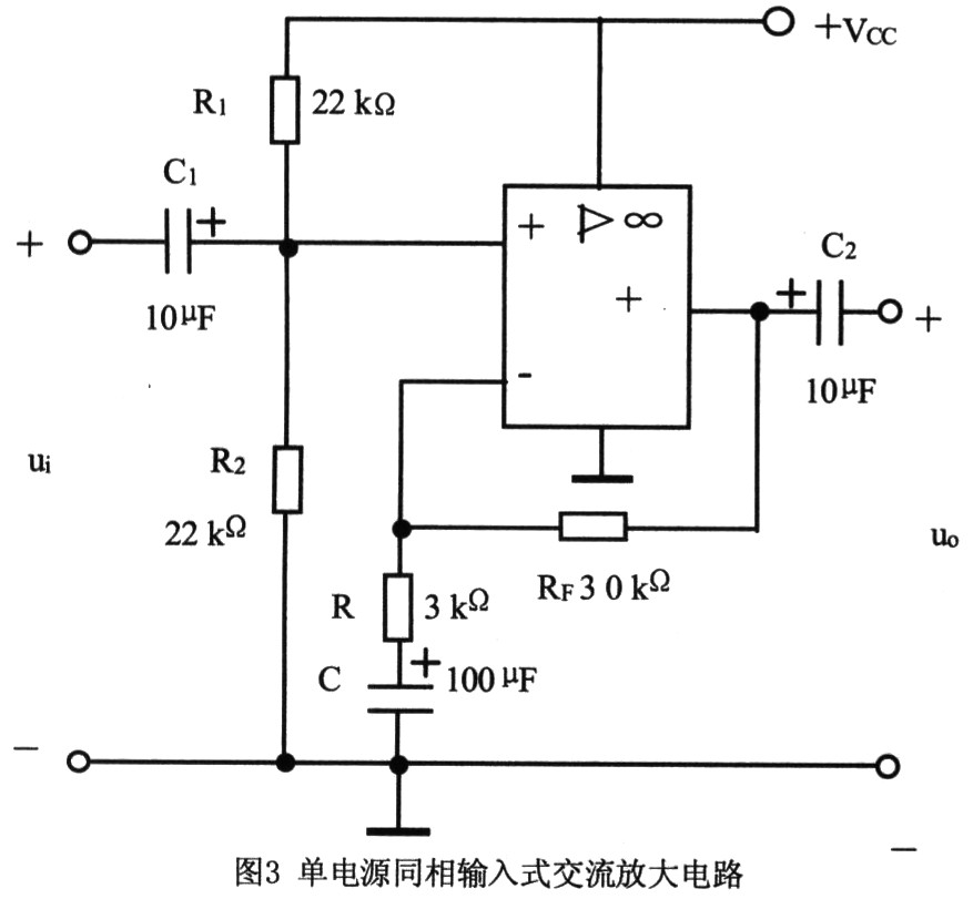
![]()
![]()
Shaft sleeve connector
Shaft sleeve connector
Material: stainless 304
Surface: ultrasonic wave cleaning, passivating
Tube connector
Material: GB20
Surface: trivalent chromium zinc coating
Application: fixed end for control system assembly
Tube guide threaded
Material: stainless 304
Surface: ultrasonic wave cleaning, passivating
Application: control system in Yacht