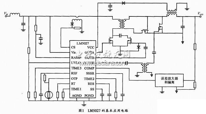
The characteristics, pin function, working principle and application circuit of the voltage type active clamp forward control IC-LM5027 are introduced in detail. The LM5027 includes many new features that, in addition to the regular functions of the basic active clamp forward circuit, adds a single-latency delay adjustment between the three output signals for better low EMI and high efficiency. Power conversion. The main features of the LM5027 pulse width modulator are: voltage type control, voltage feed forward function; internal 105V high voltage start source; adjustable undervoltage lockout; two modes of overcurrent protection; adjustable volt-second product Limit; adjustable soft start time; adjustable synchronous rectifier drive start and stop; precise 0.5V overcurrent comparator; current sense function with leading edge blanking; adjustable delay between two outputs to achieve ZVS switch. The basic application circuit of the LM5027 is shown in Figure 1. 1 pin function introduction The 20 pins of the LM5027 function as follows: 1 PIN VIN: High-voltage starting source input, input operating voltage range is 13~90V, maximum withstand voltage is 105V, LM5007 can also be directly from VCC to external bias source. 2 PIN RAMP: Voltage feedforward modulation terminal, externally connected from VIN to an RC circuit, set PWM ramp slope, discharge at the end of each cycle, if this terminal voltage exceeds 2.5V, it limits the maximum volt-second product to the transformer primary. 3 PIN TIME3: Delay adjustment, externally connected to a resistor, set the overlap delay of the main clamp output, RTIME3 resistor connected to this end to AGND, set the pulse delay of OUTA off to OUTB turn-on. 4 PIN TIME2: Delay adjustment 2, external resistors set the overlap delay of the OUTSR output, RTIME2 is connected to this terminal to AGND, set the pulse delay of OUTA to the OUTSR turn-on. 5 PIN TIME1: Delay adjustment 1, external resistor to set the overlap delay of the clamp output, RTME1 resistor connected to this end to AGND, set the overlap delay between OUTB and OUTSR turn-off to OUTA turn-on. 6 PIN AGND: Analog ground of IC, directly connected to PGND. 7 PIN RT: Oscillation frequency setting and external synchronization input. Usually the internal amplifier is biased at 2V. Externally connect a resistor to AGND to set the oscillation frequency. When the external input is higher than the internal oscillator frequency, it will be synchronized to the external frequency. 8 PIN COMP: Connected to the pulse width modulator, the external feedback optocoupler is directly connected to this terminal, and the current is input through the internal NPN current mirror. The PWM duty cycle is maximum at zero input current, which is occupied when 1mA current is input. With a null ratio of 0, the current mirror improves the frequency response. It reduces the AC voltage of the phototransistor in the optocoupler. 9 PIN REF: Outputs a 5V reference voltage source, which can supply up to 10mA current, and external 0.1μF capacitor bypass decoupling. 10 PIN OUTB: Output driver, external drive clamp MOSFET (P type) gate, the source leakage current capability is 1A. 11 PIN OUTA: Output driver, external drive power MOSFET (N-type) gate, source leakage capability of 2A. 12 PIN OUTSR: The gate of the MOSFET that controls the secondary æ» synchronous rectification, the source leakage current capability is 3A. 13 PIN VCC: The output of the IC start voltage regulator, that is, the output of the internal high voltage start source, which is 9.5V at start-up and 7.5V during normal operation. If the voltage of the external auxiliary winding is rectified slightly higher than this voltage, the internal high voltage The start source will be turned off to reduce IC power consumption. 15 PIN CS: current detection input, cycle-by-cycle current limit in the IC. If the CS terminal voltage exceeds 500mV, the IC output drive will be terminated, enter the cycle-by-cycle current limit mode, and the main output OUTA after 100 ns voltage drop at the CS terminal The switch goes high, blanking the leading edge. 16 PIN SS: Soft-start input. An internal 20μA current source charges the external soft-start capacitor at this end to set the soft-start rate. 17 PIN RES: Restart period. If the cycle-by-cycle current limit level is reached in any one cycle, a 22μA current source flows into the RES capacitor. If the RES capacitor voltage is charged to 1.0V, the hiccup mode begins, the SS and SSSR capacitors are discharged, and the controller output terminates the RES capacitor. The voltage on the voltage is dithered eight times between 4V and 2V. After the eighth time, the SS terminal capacitance is released and the normal startup sequence begins. 18 PIN SSSR: Soft start of the synchronous rectifier output. An external capacitor and an internal 25μA current source are used to set the soft-start ramp of the synchronous rectifier output (OUTSR). 19 PIN OTP: Overheat protection. The OTP comparator is used for thermal shutdown protection, and an NTC thermistor divider is externally connected to set the shutdown temperature. The OTP comparator threshold is 1.25V. When the OTP terminal voltage exceeds the threshold, the window flows from the internal current source 20μA into the external resistor divider. 20 PIN UVLO: The path is under voltage lock. The external VIN is connected to a resistor divider to set the level of the shutdown point and the standby comparator. The two regulators VCC and REF are turned off when the UVLO reaches 0.4V. When the UVLO is 2V, the SS terminal is released and the device is re-operated. The window is set by an internal current source (20μA) and an external divider resistor. 2 internal structure and function 2.1 High voltage starting source The LM5027 IC has a high voltage start regulator inside. Its VIN terminal can be directly connected to the line input voltage (100V) regulator output current is limited to 55mA, when the UVLO terminal voltage exceeds 0.4V. The VCC regulator is enabled and charged to the capacitor external to VCC. The VCC regulator supplies energy to the voltage reference REF and the three gate drive outputs. When the VCC voltage reaches 9.5V. The output of the controller is enabled and the internal reference reaches the 5V regulation point. The UVLO terminal voltage is greater than 2V. The OTP voltage is greater than 1.25V and the output drive goes into normal operation unless the UVLO is below 2V. The OTP end drops below 1.25V. The VCC capacitor value depends on the system design and startup characteristics, and the standard value is 0.1 to 100 μF. In a typical application, the transformer auxiliary winding must be able to pass the diode to VCC voltage of 2.5 to 7.5V. Powering through the auxiliary winding improves efficiency and reduces power consumption of the control IC. At this time, the high voltage starting source is turned off, and VIN and VCC can be connected together if the external power supply is directly used. 2.2 Line undervoltage detector The LM5027 has two level-detected UVLO circuits. When the UVLO is greater than 0.4.V but still below 2V, the controller is in standby mode. At this point, both VCC and REF regulators are activated, but the controller's output is also disabled. This feature allows the LM5007 to be used for remote control functions. When the UVLO is below 2V, the LM5027 enters the soft-shutdown procedure. The 0.4V shutdown comparator has a 100mV window. When the VCC and REF outputs exceed their given undervoltage threshold. The UVLO terminal voltage is also greater than 2V. When the OTP terminal voltage is greater than 1.25V, the controller output is enabled. Enter normal work. An external resistor divider is connected from VIN to GND to set the minimum operating voltage. The UVLO at this time must be greater than 2.0V. If this value is met, all three outputs are disabled. The UVL0 window is determined by an internal 20μA current source. 2.3 Cycle-by-cycle current limit The CS terminal is driven by a representative signal of the primary current of the transformer. If the voltage at the CS terminal exceeds 0.5V. The current sense comparator terminates the three output drive pulses. The duty cycle depends on the comparator, instead of the PWM comparator, a small RC filter is connected to the CS terminal to suppress noise. The internal 5Ω MOSFET will discharge the charge on the CS external capacitor at the end of each cycle. Before the OUTA driver switch is high for 30ns. The inside of the discharge MOSFET is in an on state. The leading edge transient of the blanking current detection circuit. In each cycle, the CS terminal discharges, blanking the leading edge spikes can reduce the need for filtering and improve the response time of current sensing. The current sense comparator operates very fast. And respond quickly during the noise pulse.
Kara offers a range of Rotary Switches.Ranging from 5 to 9 poles,15VA to 25 amp,with many choices of functions,especially the switches with High-Current .Certifications include CSA, CE, and more.
This item used very in the line of cooler,with metal panel or plastic panel or only switch are all available.
Rotary Switch,Rotary Switch Knobs,Rotary Switch 6 Position,Mini Rotary Switch Ningbo Kara Electronic Co.,Ltd. , https://www.kara-switch.com