The semiconductor lighting industry is facing a rare historical opportunity. The output of LED packaging and application products in China has accounted for 70% of the world's total. The development of the LED industry is taking advantage of the development of the LED industry. It is actively developing in the direction of advantages, promoting technological progress and maturity of production processes, thus promoting China's semiconductor industry. The overall advancement of lighting technology has also played a crucial role in the arrival of the era of semiconductor lighting.
Thick Copper PCB are used extensively in power electronic devices and power supply systems. A growing trend in the PCB industry, this unique type of Heavy Copper PCB features a finished copper weight of more than 4oz (140μm), compared to the 1oz (35μm) or 2oz (0μm) copper weight generally found in those with a Standard PCB copper thickness.
PCB Manufacture Capabilities
Features
Capabilities
Layers
1-36 layers
Material
FR-4, Aluminum, Copper, Polyimide, high frequency (Rogers, PTEE, PI), etc.
PCB Type
FR-4 Standard PCB, Aluminum PCB , Copper-based PCB, HDI PCB , Rigid-Flex PCB, Flex PCB, Thick copper PCB and Rogers PCB, etc.
Board Thickness
0.1mm-6.0mm
Copper Thickness
1/2oz-6oz(18um-210um)
Biggest Board size
600mm*1200mm
Min Tracing/Spacing
0.075mm/0.075mm (3mil/3mil)
Min drilling Hole diameter
0.15mm(6mil), 0.1mm(4mil)-laser drill
Solder Mask
Green, Black, White, Red, Yellow, Blue and Purple, etc.
Silkscreen color
White, Blue, Black, Red, Yellow
Surface finish
HASL Lead free, Immersion Gold (ENIG), Immersion Tin, Immersion Silver, OSP, Carbon oil, etc.
Special Techniques
Impedance Control, Gold Fingers, Blind/Buried vias, Peelable solder mask, Half holes, Via-in-Pad and Countersink hole, etc.
PCB Products Show
PCB Factory Show
Thick Copper PCB Thick Copper PCB,Thick Copper PCB Board,Copper Thickness Tester PCB,Quality Thick Copper PCB ZhongFeng Electronic Technology Co., Limited , https://www.dopcba.com
On August 30th, the 8th High-tech LED Industry Summit held in conjunction with the High-tech LED Boutique Exhibition was held in the Century Hall of the Shanghai International Convention Center. The technical section of the forum revolves around "LED Lighting Technology - Problems and Solutions", LED lighting design and application engineering - the theme of deciding the segmentation field, etc. The sapphire production process in the whole industry chain of LED, middle and lower reaches, LED epitaxial chip technology at home and abroad, phosphor, detection equipment, LED devices and modules, and OLED From the point of view to the topic, I shared a comprehensive key technology with the guests. Participants expressed that it was a very rare training and promotion opportunity.
Dr. Chen Wencheng, program manager of OSRAM Opto Semiconductors Asia Ltd. believes that the development trend of package structure will be smaller and smaller package size (3mm*3mm), and the chip size is getting larger and larger. Future packaging methods will move in the direction of 351, 5630. Regarding the standard of the LED shooting light engine, it stipulates that there is no need for the LED packaging method inside the tube, and there are standardized mechanical interfaces, heat dissipation, drive systems, and optical systems. One advantage of the LED device itself is that it can be 300LM or 500LM, and there is no need to use the light engine for lumens at this stage. Light efficiency with high power lumens is the highest and performance is the most stable. The disadvantages are inconvenient to process and require the support of many engineers. The biggest advantage of modules and light engines is that they save time in research and development. But only by standardizing the way, the light engine and modularity will have a better development direction. 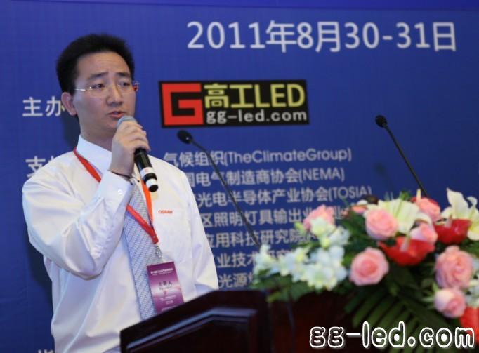 Â
 ![]()
The additional copper PCB thickness enables the board to conduct a higher current, achieve good thermal distribution and implement complex switches in a limited space. Other advantages include increased mechanical strength at connector sites, the ability to create a smaller product size by incorporating multiple weights on the same layer of circuitry and the ability to use exotic materials to their maximum capacity with minimal risk of circuit failure.

