The electronic load machine is a must-have tool for many friends who are engaged in the design of electric power, especially power supply design and production. In the design, it is sometimes necessary to discharge the battery and other devices. If a cement resistor is used to carry out the current, not only the constant current is not enough. Convenient, and buy a finished electronic load machine on the market, the cheapest is also nearly 1,000 yuan. The author made an electric load machine by himself. The production components of the load machine are easy to find, can be used without debugging after production, and have constant current and various protection functions. After the trial effect is very satisfactory, it can be used not only for constant current discharge of the battery, but also for aging experiments on the power products produced by the factory. Here's how to share it with everyone.
Circuit principle
The circuit is shown below. VT4 provides a 2.5V reference for the entire circuit. IClA, R9, VT1, VT2, etc. constitute a switching constant current circuit. For example, when the load terminal is connected to the battery, and the voltage drop generated at the beginning of the current on R9 (point C) is not high at point B, the output of point D is high, and VT1 and VT2 are continuously turned on, so on R9. The voltage drop (point C) will continue to increase until the voltage at point B is exceeded. At this point, the output of point D is low, and VT1 and VT2 are turned off. This process is repeated, so the constant current = {[2.5 ÷ (R7 + R8)] × R8} ÷ R9. Taking the figure as an example, the current flowing through the L0ad terminal is {[2.5÷(100k+10k)]×10}÷O.1≈2.3A.
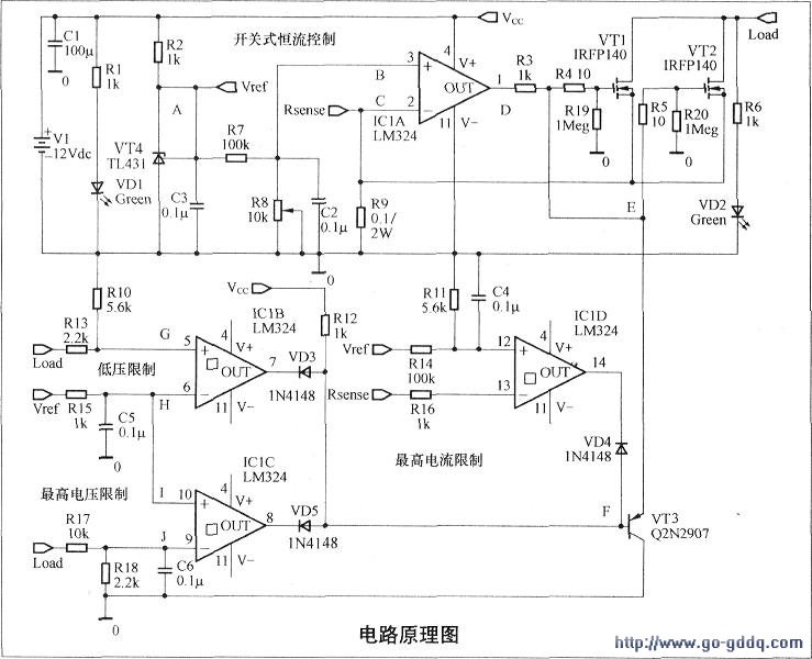
IC1B acts as a low voltage protection. Usually, the G point potential is higher than H point, so the F point is high, VT3 does not work, and VT1 and VT2 work normally. When the voltage of the load terminal is lower than the set value, the F output is L, VT3 acts, the driving voltage of VTl, VT2 (point E) is pulled low, VTl, VT2 will not conduct, no load current flows through the load port, Low pressure protection. For example, when discharging a lead-acid battery, when the 12V battery is placed at a voltage of only 3V, the circuit will exert a low-voltage protection function to terminate the discharge current. The discharge voltage desired to be terminated can be calculated by [U ÷ (R13 + R10)] × R10 = 2.5 V, where U is the discharge voltage desired to be terminated.
The role of IClC is the highest voltage limit, the principle is the same as IClB, it is used to protect VT1, VT2 safe work. Imagine that the current flowing through VT1 and VT2 is constant. When the voltage at the load terminal rises unrestrictedly, the power consumption of VT1 and VT2 increases without limit, and the power consumption of VT1 and VT2 is limited. VT1, VT2 are likely to be damaged, so the maximum voltage limit must be made.
IC1D acts as the maximum current limit, and the principle is the same as IClC. When the R8 adjustable resistor in the above figure is open, the voltage at point B is 2.5V. At this time, the current limit value is 25A, and VT1 and VT2 must be damaged if the power consumption is insufficient. This part of the formula is: the maximum limit current that wants to flow through R9: {[2.5÷(R14+R11)]×R11}÷R9.
Production Method
The circuit is made of common components, but VT4 is very important for current limiting accuracy. It is best to choose 1% accuracy. Among them, R8, R10, R18, and R1l can all use adjustable resistors to achieve your different needs. However, it should be adjusted to the appropriate position during production to avoid unnecessary troubles in the later stages of production. In principle, the smaller the Rds(on) is, the better the VT1 and VT2 are selected, but do not force it. The standard can be lowered according to your discharge current demand.
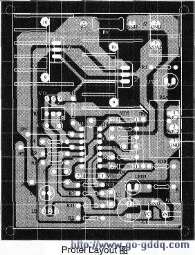
When the current at the load side flows through VT1 and VT2, these two components are prone to generate high heat. For example, when the voltage at the load terminal is 12V, if the current flowing through R9 is 2A (R8 ≈ 8.5kΩ), VT1 and VT2 will respectively generate power consumption of about 11.7w. If the voltage at the load terminal is 24V, power consumption of about 24w will be generated separately, so it is strongly required to add a sufficiently large heat sink to VT1 and VT2 at the time of fabrication. In addition, if you do not have enough power MOSFET, you can limit the maximum current flowing through VT1 and VT2 by adjusting the value of R11 to protect them safely and reliably. An ammeter can be connected to the Load to facilitate monitoring of the current. The picture on the right is the board made by the author for reference. In addition, if you need Protel circuit diagram and Layout diagram of this circuit, or friends of PSpice simulation model, you can download it from our website.
Photo Studio Kit,Photography Lighting Kit,Photography Studio Kit,Photography Studio Lighting Kit
SHAOXING SHANGYU FEIXIANG PHOTOGRAPHIC CO.,LTD , https://www.flying-photography.com