Thin film passive devices in radio frequency / microwave circuits Not long ago, most microwave capacitors were based on multilayer ceramic firing technology. In the production process, multiple layers of highly conductive metal alloy electrode layers and low-loss ceramic insulating layers are staggered to obtain the required capacitance value. Then, the synthesized laminate is fired at a high temperature and sintered into a monolithic structure. This process still meets the needs of large-capacity RF capacitors and high-power capacitors. Figure 1 Structure of film capacitor Figure 2 S21 forward transmission loss characteristic curve Manufacturers choose thin film capacitor components, not only to obtain the superior electrical performance of single-layer capacitors, but also to enjoy the convenience of MLCC type component applications. Fig. 3 shows the influence of the stability of the performance of the thin film capacitor on the thickness of the electrode and the oxide layer, and the influence of its quality on the K value of the insulating layer. Figure 3 Compared with MLCC, the frequency response of film capacitors has excellent repeatability Compared with air core inductors, thin film inductors have many practical advantages (although they cannot achieve the same Q value). In the surface mounting process, thin film inductors are easier to grasp and place than air core inductors. It is also very convenient to apply IR, steam phase method and wave technology which are commonly used in assembly at present. In addition, the thin-film inductor can keep the inductance value unchanged during these processes and in handling and strong vibration environments. Although they cannot be tuned in a circuit like an air core inductor, once the exact inductance value needed to achieve a certain circuit function is determined, a thin film inductor can be used instead of the air core inductor (assuming that the Q value can meet the needs). Similar to the case of thin film capacitors, the ESR and loss of thin film inductors are significantly reduced, thanks to line width control and the quality / precision of the insulation layer deposition. This allows the size of the finished product to be reduced to 0402 packages, and can achieve almost any required inductance value, while the tolerance accuracy is close to 0.05nH. In addition, the stable metallization process makes the thin film inductors have a high current carrying capacity: the current carrying capacity of different products differs, up to 1000mA. Automotive Fug Wire Tap,Fuse Tap Adapter,Cor Add A Circuit Fuse Tap,Inline Fuse Holder Dongguan Andu Electronic Co., Ltd. , https://www.autoido.com
However, the multi-layer ceramic process may lead to differences in certain parameters of different batches of products and different products of the same batch, and these parameters are very important for RF designers, such as Q value, ESR, insulation resistance And the capacitance value changes within the specified tolerance range. Although in many applications, these parameter changes will not have a negative impact, the current technological breakthrough in the field of thin-film component production is that designers provide an alternative solution for the production of high-frequency microwave components.
The thin film technology used in the production of semiconductors can also be used to produce thin film passive components with strict electrical and physical characteristics. Line width and insulation layer thickness can reach 1μm and 10nm respectively.
Strict line width dimensions bring strict parameter tolerances (inductance and capacitance values). In addition, several other electrical performance advantages can be further optimized. Due to the high vacuum electrode deposition process, the ESR values ​​between different batches of products and between different products in the same batch are extremely stable. The ultra-pure, low-K insulating layer obtained by chemical vapor deposition (CVD) makes the Q and ESR values ​​very stable. The impedance value has stability and predictability in a wide frequency range. The planar grid array (LGA) packaging process enables it to reduce parasitic parameters.
These performance advantages of thin-film components have an impact on the design. Generally, for realizing a specific circuit function, the number of required components can be reduced. By reducing the number of components used, not only will the design size be reduced, but also assembly time and assembly costs will be reduced, while product reliability will be improved. In addition, because the electrical performance of the component is more stable and the loss is lower, the overall electrical performance of the product using this component will also be improved.
Example: Band rejection filter Band rejection filter is a practical application of thin film components. The circuit design of the band stop filter is to prevent the passage of signals in a specific radio frequency spectrum and allow other signals to pass through without attenuation. It is also often referred to as a notch filter, band stop filter or band suppression filter. Band rejection filters are often used between the power amplifier and the matching circuit in front of the antenna.
Take a typical application as an example. Complex, wide-coverage multi-band radio receivers often accidentally generate difference frequencies and harmonics, and narrow-band notch filters are used to attenuate these difference frequencies and harmonics. Due to the near-perfect characteristics of the film, the use of a high-quality film capacitor can replace the six components used in the double T-shaped design.
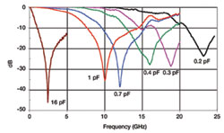
The film capacitor (shown in Figure 1) also has a performance advantage not mentioned before: its response is only one resonance point, because this device uses a single insulating layer design packaged into a multilayer ceramic capacitor (MLCC). Fig. 2 shows the forward transmission loss characteristic curve of part S21 of this film capacitor. 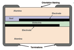

We must realize that film capacitors have limitations as band-stop filters. Because film capacitors usually provide only small capacitance values, they are limited to band-reject filter designs with relatively high frequencies. If low frequency design is involved, other filter methods must be used, usually using high-Q multilayer RF capacitors.
Thin film inductors can be used for frequency compensation of broadband amplifiers. Previously, a resistor / inductor combination was used. As in the case of thin film capacitors, the use of thin film inductors can reduce the number of components used in the circuit, thereby reducing the size of the finished product, reducing weight, simplifying assembly, reducing costs, and improving reliability.
Like thin film capacitors, thin film inductors can only provide a small inductance value, so there are limits to their application.
In other words, thin film inductors can provide designers with a good solution at very high frequencies. A common application example is an oscillator with a frequency of up to several gigahertz. At high frequencies, the use of wire-wound inductors is unrealistic because the current technology for producing wire-wound inductors with such small inductance values ​​is not yet available.
In this application, the designer has only two options: use the circuit design of the serpentine trace of the PCB circuit board to obtain low inductance, or choose a miniature surface-mount thin film inductor.
Other thin-film components use the knowledge and process capabilities gained from manufacturing thin-film capacitors and thin-film inductors. Many other components have been developed, including couplers and harmonic low-pass filters.