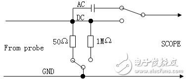
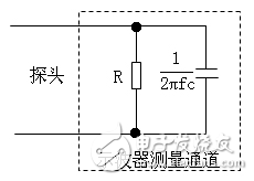
We can simply equivalent the probe model to an R, L, and C circuit, and put this model together with the circuit under test, as shown in the following figure: As shown in the figure above, Rprobe is the input resistance of the probe. In order to minimize the influence of the probe on the circuit under test, the input resistor Rprobe of the probe itself should be as large as possible, but Rprobe is impossible to achieve infinity, so it will be The measuring circuit generates a partial pressure such that the measured voltage is smaller than the actual voltage. In order to avoid the impact of the probe resistance load, Rprobe is generally required to be more than 10 times larger than Rsource and Rload. Most probes have input impedances ranging from tens of K ohms to tens of mega ohms. Cprobe is the input capacitance of the probe itself. This capacitor is not intentionally made, but the parasitic capacitance of the probe. This parasitic capacitance is also the most important factor affecting the probe bandwidth because it attenuates high frequency components and slows the rising edge of the signal. Usually the high bandwidth probe parasitic capacitance is relatively small. Ideally Cprobe should be 0, but it can't be done. Generally, the input capacitance of a passive probe is between 10pf and several hundred pf, and the active probe input capacitance of a higher bandwidth is generally between 0.2pf and a few pf. Lprobe is the parasitic inductance of the probe lead. Usually, the ground of the 1mm probe will have an inductance of about 1nH. The longer the signal and ground, the larger the inductance. The parasitic inductance and parasitic capacitance of the probe constitute a resonant circuit. When the inductance value is too large, high frequency resonance may occur under the excitation of the input signal, causing signal distortion. Therefore, it is necessary to strictly control the length of the signal and the ground line during high-frequency testing, otherwise it is easy to generate ringing. When using the oscilloscope, you need to set the coupling mode and input impedance of the oscilloscope measurement channel. The coupling modes are AC and DC. The input impedance is 1MΩ and 50Ω. There are many types of probes for oscilloscopes, but the oscilloscope's matching is always only 1M ohm or 50 ohm. Different types of probes need different resistors to match. The circuit diagram of the oscilloscope input interface is shown below: When measuring ordinary signals, DC coupling is generally used. When measuring the ripple/noise of the power supply, AC coupling is required. When the oscilloscope is connected to the active probe, the input impedance is automatically switched to the 50Ω position. When connecting the passive probe, you need to manually switch to 1MΩ gear. From the point of view of voltage measurement, in order to reduce the influence on the circuit under test, the oscilloscope should use a high input impedance of 1 MΩ, but the bandwidth of the high-impedance circuit is easily affected by the parasitic capacitance. So 1MΩ input impedance is widely used in measurements below 500M bandwidth. For higher frequency measurements, a 50Ω transmission line is typically used, so an oscilloscope 50 ohm match is primarily used for high frequency measurements. To better illustrate the effects of oscilloscope input impedance and parasitic capacitance on the measurement channel bandwidth, we convert the circuit diagram from the time domain to the frequency domain, as shown in the following figure: As shown in the figure above, the equivalent impedance of the parasitic capacitance of the oscilloscope input channel is 1/(2πfc). In the low frequency case, the value of 1/(2πfc) is very large, no current flows through C, and the input impedance of the oscilloscope is equal to the value of R. However, as the signal frequency increases, the equivalent impedance of the parasitic capacitance 1/(2πfc) becomes smaller and smaller. Therefore, under high-frequency signals, the parasitic capacitance has a great influence on the input impedance of the oscilloscope. Is R//[1/(2πfc)]. In order to reduce the influence of parasitic capacitance on the input impedance of the oscilloscope under high-frequency signals, the input impedance of the oscilloscope is set to 50Ω when testing high-frequency signals.
We've been around for over 16+ years. We make sure our sound is The Best Sound.
Manufacturing high-quality products for customers according to international standards, such as CE ROHS FCC REACH UL SGS BQB etc.
wholesale earbuds, earbuds in bulk, earbuds custom, true wireless earbuds TOPNOTCH INTERNATIONAL GROUP LIMITED , https://www.itopnoobluetoothes.com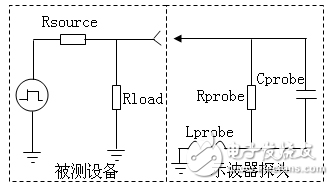
Oscilloscope probe circuit diagram and its schematic diagram
First, the oscilloscope probe circuit diagram