Before learning a technology, we often start with its programming language. For example, when learning a microcontroller, we often get started with assembly or C language. So many developers who start to contact FPGAs often start with VHDL or Verilog. But I personally think that if you can learn all kinds of 74 series logic circuits in combination with the "Digital Circuit Fundamentals" system, and deeply understand the logic function, it will be beneficial to the learning of HDL language, and it will often have a multiplier effect. Of course, the learning of any programming language is not a one-off event. The accumulation of experience and skills is done in a little bit, and FPGA design is no exception. Let me take a look at my experience and skills in FPGA design. Let's talk about the basics of FPGA first: FPGA (Field-Programmable Gate Array), which is a field-programmable gate array, is a product further developed on the basis of programmable devices such as PAL, GAL, and CPLD. It emerged as a semi-custom circuit in the field of ASICs, which not only solves the shortcomings of custom circuits, but also overcomes the shortcomings of the limited number of gates of the original programmable devices. 1, the basic principles of hardware design (1) Speed ​​and area balance and interchange principle: If a design has a large timing margin, the frequency that can be run is much higher than the design requirements, and the module can be reused to reduce the chip area consumed by the entire design. Speed ​​advantage for area saving; conversely, if the timing requirements of a design are very high and the common method does not reach the design frequency, then multiple operation modules can be copied in parallel through data stream and conversion, and "ping-pong operation" is adopted for the entire design. And the idea of ​​"serial-to-parallel conversion" is processed, and the data is "parallel-serial conversion" at the chip output module. Thereby, the improvement of the area copying exchange speed is realized. (2) Hardware principles: understanding the nature of HDL (3) System principle: overall grasp (4) Synchronous design principle: the basic principle of designing time series stability 2. Verilog, as an HDL language, models the behavior of the system in a hierarchical manner. The more important levels are system level, algorithm level, register transfer level, logic level, gate level, and circuit switching level. 3. In actual work, except for the use of for loop statements in describing the simulation test stimulus, the for loop is rarely used in RTL-level coding. This is because the for loop is expanded by the synthesizer into execution statements for all variables, each variable. Independently occupying register resources, can not effectively multiplex hardware logic resources, resulting in huge waste. Commonly used case statements instead. 4, if...else... and case are very different in nested description, if...else... is prioritized, in general, the first if has the highest priority, and the last one has the lowest priority. . The case statement is a parallel statement, it has no priority, and the establishment of the priority structure requires a lot of logic resources, so you can not use the if...else... statement in the case of the case. Supplement: 1. You can also use if...; if...; if...; to describe a "parallel" statement without precedence. 5, FPGA general trigger resources are relatively rich, and CPLD combination logic resources are more abundant. 6, the composition of FPGA and CPLD: FPGA basically consists of programmable I/O unit, basic programmable logic unit, embedded block RAM, rich routing resources, underlying embedded functional unit and embedded dedicated hard core. The structure of the CPLD is relatively simple, and is mainly composed of a programmable I/O unit, a basic logic unit, a wiring pool, and other auxiliary function modules. 7, Block RAM: 3 block RAM structures, M512 RAM (512bit), M4K RAM (4Kbit), M-RAM (64Kbit). M512 RAM: suitable for some small Buffer, FIFO, DPRAM, SPRAM, ROM, etc.; M4K RAM: for general needs M-RAM: A buffer suitable for making large blocks of data. The LUTs of Xlinx and Lattice FPGAs can be flexibly configured into small RAM, ROM, FIFO and other storage structures. This technology is called distributed RAM. Supplement: However, in the general design, it is not recommended to use FPGA/CPLD's on-chip resources to configure a large amount of memory, which is a cost consideration. So try to use external storage. 8. Make good use of the internal PLL or DLL resources to complete the clock frequency division, double frequency, and shift equal operation, which not only simplifies the design, but also effectively improves the accuracy and stability of the system. 9, the difference between asynchronous circuit and synchronous sequential circuit Asynchronous circuit: The circuit core logic is implemented by a combination circuit; The biggest disadvantage of asynchronous sequential circuits is that they are prone to burrs; Not conducive to device migration; Not conducive to static timing analysis (STA), verify design timing performance. Synchronous timing circuit: The circuit core logic is implemented with various triggers; The main signal, output signal, etc. of the circuit are generated by driving the trigger on a certain clock edge; Synchronous timing circuit can avoid burrs very well; Conducive to device transplantation; Conducive to static timing analysis (STA), verify design timing performance. 10. In synchronous design, stable and reliable data sampling must follow the following two basic principles: (1) Before the effective clock edge arrives, the data input has at least stabilized the setup time of the sampling register. This principle is referred to as the Setup time principle for short; (2) After the valid clock edge arrives, the data input will at least keep the Hold clock of the sample register stable for a long time. This principle is referred to as the Hold time principle. 11, synchronization timing design considerations: Data conversion for asynchronous clock domains. The design method of the combinational logic circuit. The clock design of the synchronous timing circuit. The delay of the synchronous timing circuit. The most common design method for delays in synchronous sequential circuits is to use a divided or multiplied clock or a synchronous counter to achieve the required delay. In contrast to the larger and special timing required delays, a high-speed clock is typically used to generate a counter, based on the count. A delay is generated; for a relatively small delay, a D flip-flop can be used, which not only delays the signal by one clock cycle, but also completes the initial synchronization of the signal with the clock. Used in input signal sampling and adding timing constraint margins. In addition, there is a behavior-level method to describe the delay, such as "#5 a"=4'0101;" which is often used to simulate test excitation, but it is ignored in circuit synthesis and does not play a role in delay. The reg types defined by Verilog are not necessarily integrated into registers. The two most commonly used data types in Verilog code are wire and reg. In general, the data and network lines specified by the wire type are implemented by combinatorial logic, and the data specified by the reg type is not necessarily implemented by registers. Open the door of the "Industry 4.0 + Internet of Things" ecological chain! What are you waiting for in the torrent of the Internet of Things! "How can you miss this new feast of the Internet of Things?! The third "China IoT Conference" organized by Huaqiang Jufeng's Electronic Enthusiasts Network will be held in Shenzhen on December 2: Global Vision The exclusive view of higher value, more professional technology sharing, more cutting-edge pulse grasp, and the gathering of well-known enterprises and elites of the global Internet of Things, you must not miss it! For more information, please continue to pay attention to the electronic enthusiast network!" (Click on the picture see details) 12, common design ideas and skills (1) ping-pong operation; (2) serial-to-parallel conversion; (3) Pipeline operation; (4) Asynchronous clock domain data synchronization. It refers to the problem of how to reliably exchange data between data fields where two clocks are not synchronized. There are two main situations in which the data clock domain is out of sync: The clock frequencies of the two domains are the same, but the phase difference is not fixed, or the phase difference is fixed but unmeasurable, which is simply referred to as the same-frequency out-of-phase problem. The two clock frequencies are fundamentally different, referred to as the inter-frequency problem. Two methods of asynchronous clock domain operation that are not recommended: one is to adjust the sampling by increasing the Buffer or other gate delay; the other is to blindly use the positive and negative edges of the clock to adjust the data sampling. 13, the basic principles of module division: (1) Use the register for the output of the submodule designed for each synchronous timing (using the register to divide the synchronous timing module principle). (2) Divide the relevant logic and the logic that can be reused into the same module (corresponding to the system principle). (3) Separate the logic of different optimization goals. (4) The logic that sends the constraint is assigned to the same module. (5) The storage logic is divided into modules independently. (6) Appropriate module size. (7) The top-level module is preferably not logically designed. 14, the considerations of combinatorial logic (1) Avoid combinatorial logic feedback loops (easy to glitch, oscillate, timing violations, etc.). solve: A. Keep in mind that any feedback loop must contain registers; B. Check the comprehensive and realize the warning information of the report, and find the feedback loop (combinational loops) and modify accordingly. (2) Replace the delay chain. Solution: Complete with multiplier, crossover or sync counter. (3) Replace the asynchronous pulse generating unit (burr generator). Solution: Design the pulse circuit with synchronous timing. (4) Use the latch with caution. solve: A, use a complete if...else statement; B. Check whether the combination logic feedback loop is included in the design; C. Design an output operation for each input condition and set the default operation for the case statement. Especially in state machine design, it is best to have a default state transition, and each state preferably has a default operation. D. If you use a case statement, especially when designing a state machine, try to add a comprehensive constraint attribute as a full conditional case statement. Tip: Check the comprehensive report of the synthesizer carefully. At present, most of the synthesizers will report “warning†to the integrated latch. It is more convenient to find out the inadvertently generated latch through the comprehensive report. 15, the clock design considerations (1) Recommended clock design method for synchronous timing circuit: The clock is input through the global clock input pin, and is divided/multiplied, shifted, equalized and operated by a dedicated PLL or DLL inside the FPGA, and then driven by the internal global clock routing resource of the FPGA to reach the clock input of all registers and other modules in the chip. end. The five basic functions of the FPGA designer: simulation, synthesis, timing analysis, debugging, and verification. For FPGA designers, practicing these five basic skills is the same process as using the corresponding EDA tools. The corresponding relationship is as follows: 1. Simulation: Modelsim, Quartus II (Simulator Tool) 2. Comprehensive: Quartus II (Compiler Tool, RTL Viewer, Technology Map Viewer, Chip Planner) 3. Timing: Quartus II (TimeQuest Timing Analyzer, Technology Map Viewer, Chip Planner) 4, debugging: Quartus II (SignalTap II Logic Analyzer, Virtual JTAG, Assignment Editor) 5. Verification: Modelsim, Quartus II (Test Bench Template Writer) Mastering the HDL language is not all of the FPGA design, but the impact of the HDL language on the FPGA design runs through the entire FPGA design flow, which is complementary to the five basic functions of the FPGA design. For FPGA designers, using the "integratable subset of HDL language" can accomplish 50% of the FPGA design work - design coding. The three basic skills of simulation, synthesis, and time series analysis are helpful for learning the "integratable subset of HDL language": 1. Through simulation, you can observe the logical behavior of HDL language in FPGA. 2. Through synthesis, you can observe the physical implementation of HDL language in FPGA. 3. Through the timing analysis, the physical realization characteristics of the HDL language in the FPGA can be analyzed. For FPGA designers, using the "HDL language verification subset", you can complete another 50% of the FPGA design - debugging verification. 1. Set up the verification environment, and verify the correctness of the FPGA design through simulation. 2, comprehensive simulation verification can reduce the workload of FPGA hardware debugging. 3. Combine the hardware debugging and simulation verification methods, use the debugging to solve the unverified problems of the simulation, and use the simulation to ensure that the solved problems are not reproduced in the debugging. A regression verification process can be established to help maintain the FPGA design project. The five basic functions of the FPGA designer are not isolated and must be combined to complete a complete FPGA design flow. Conversely, by completing a complete design process, you can practice these five basic skills most effectively. With a preliminary understanding of these five basic skills, you can learn some of them in depth and then reuse the knowledge you have learned in the complete design process. Repeatedly, you can gradually improve the design level. With such a step-by-step, spiral-up approach, as long as you enter the door through training, you can self-study and self-improve. Books on FPGA design sold in the market are designed to ensure the integrity of the structure. Each aspect of the FPGA design is introduced separately. Although each aspect is in-depth, due to the lack of support from other related parties, it is difficult for readers to put into practice. A complete book can gain a holistic view of FPGA design. Such a book, as an engineering training guide, can not be used as an advanced reference book for a certain aspect. For new employees, they often have a preliminary understanding of the overall design process of the FPGA, and some aspects of the five basic skills may be solid. However, the lack of ability in one or a few aspects limits their ability to complete the entire design process on their own. The purpose of on-the-job training is to help them master the overall design process, cultivate their ability to acquire information, and train back and forth through several design processes to form a virtuous cycle of self-promotion and self-development. In this process, as the understanding of the breadth and depth of the knowledge involved in the work is gradually clear, the self-confidence of new employees will gradually increase, and the direction of personal development will be gradually clear, so that they can actively participate in the project. Come in. Finally summarize the points: 1) Look at the code and build the model Only by establishing a logical model in the mind and understanding the basics of the internal logic structure of the FPGA can you understand why the whole idea of ​​writing Verilog and writing C is different, in order to understand the difference in the design method of sequential execution language and parallel execution language. . What kind of functional circuit should I think of when I see a simple program. E.g: 2) Use mathematical thinking to simplify design logic Learning FPGA is not only important for logical thinking, but good mathematical thinking can also make your design simple, so ah, those children who see headaches when they see high numbers need to pay attention to this course. For a simple example, for example, there are two 32-bit data X[31:0] multiplied by Y[31:0]. Of course, both Altera and Xilinx have ready-made multiplier IP cores to call, which is the easiest way, but two 32-bit multipliers will consume a lot of resources. So is there any way to save resources and not to do it in a complicated way? We can make a slight modification: Split X[31:0] into two parts X1[15:0] and X2[15:0], let X1[15:0]=X[31:16], X2[15:0]=X[15 :0], X1 is shifted to the left by 16 bits and then added with X2 to get X; likewise, Y[31:0] is split into two parts Y1[15:0] and Y2[15:0], let Y1[15: 0]=Y[31:16], Y2[15:0]=Y[15:0], then Y1 is shifted to the left by 16 bits and then added with Y2 to get Y; then the multiplication of X and Y can be converted into X1. And X2 are multiplied by Y1 and Y2, respectively, so that a 32bit*32bit multiplication is converted into four 16bit*16bit multiplication operations and three 32bit addition operations. After the conversion, the occupied resources will be reduced a lot. Interested children's shoes, may wish to take a look at it and see how much the difference is. 3) Relationship between clock and trigger "The clock is the controller of the sequential circuit" is too classic, it can be said that the design of FPGA design. The design of FPGA is mainly based on sequential circuits. Because the complex logic circuit is no longer complicated, it can not change too many patterns, and it is not too difficult to understand. But the timing circuit is different. All its actions are triggered by the clock at the beat of the beat. It can be said that the clock is the controller of the whole circuit. If the control is not good, the circuit function will be chaotic. For example, the clock is equivalent to the heart of the human body. Each time it beats, it triggers a CLK to supply blood to various organs of the body, maintaining the normal operation of the body. Every organ system works normally and the composition of tissue cells is indispensable. The device can be compared to the basic unit tissue cells. The clock of the sequential logic circuit is the "engine" that controls the state transition of the sequential logic circuit. Without it, the sequential logic circuit can not work normally, because the sequential logic circuit mainly uses the state of the flip-flop to store the circuit, and the trigger state transition requires the clock to rise. Or falling edge! This shows the core role of the clock in the sequential circuit! Finally, let’s talk about the experience. It comes down to practice, think more, and ask more. Practice the truth, look at the 100-person solution is not as good as you can. The driving force of practice comes from interest on the one hand and pressure from the other. I personally think that the latter is more important. There is a need to create pressure on the demand, which means that it is best to exercise in the actual project development, rather than learning for learning. In the process of practice, you should think more, think about the cause of the problem, and ask a few more questions after the problem is solved. This is also the process of accumulation of experience. If there is a habit of writing a project log, it is better to solve the problem and cause the problem. The methods are written in. In the end, I have to ask more questions. After I have encountered problems and think about it, I have to ask. After all, personal strength is limited. Ask colleagues and colleagues, ask search engines, ask netizens, and an article, friends’ call. They may help themselves solve problems quickly. Mining is the process of creating a block of transactions to be added to the Ethereum blockchain in Ethereum's now-deprecated proof-of-work architecture.
Mining is the lifeblood of any proof-of-work blockchain. Ethereum miners - computers running software - used their time and computation power to process transactions and produce blocks prior to the transition to proof-of-stake.
ETH Miner:Antminer E9 2.4Gh/S,Bitmain E9 2.4Gh/S,Bitmain Antminer E9 2.4Gh/S
Eth Miner ,Antminer E9 2.4Gh/S,Bitmain E9 2.4Gh/S,Bitmain Antminer E9 2.4Gh/S Shenzhen YLHM Technology Co., Ltd. , https://www.asicminer-ylhm.com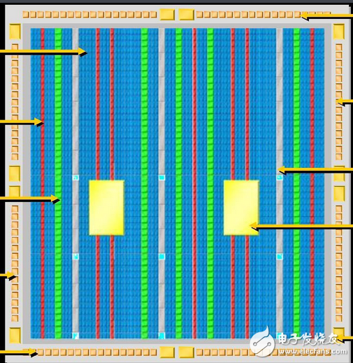
The word mining originates in the context of the gold analogy for cryptocurrencies. Gold or precious metals are scarce, so are digital tokens, and the only way to increase the total volume in a proof-of-work system is through mining. In proof-of-work Ethereum, the only mode of issuance was via mining. Unlike gold or precious metals however, Ethereum mining was also the way to secure the network by creating, verifying, publishing and propagating blocks in the blockchain.
Mining ether = Securing the Network