Power Supplies Power Supplies,Portable Power Station 200W,Super Portable Power Station,Portable Solar Generator Lithium Inverter GuangZhou HanFong New Energy Technology Co. , Ltd. , https://www.hfsolarenergy.com
When considering an integrated circuit, today's design engineers look for low-power features as well as performance. Saving a few milliamps of quiescent current per chip may seem trivial, but it becomes substanTIal for a board with dozens of ICs. Such savings allow the use of smaller power supplies and less power drawn from the wall outlet. For small, portable, battery-operated devices, power savings allow longer operaTIon from the battery.
With low-power CMOS processes and intelligent power management, the operating time for today's portable devices has become remarkably long. Supply voltage has also decreased dramatically over the last few years. Many designs now run with a 3.3V main supply or directly from a single Li + cell! Semiconductor manufacturers have been very creative in meeting all requirements of the ubiquitous RS-232 standard with these low voltages. But, compromises are now necessary to save even more current. This article shows how to run the interface at the lowest possible power by seeking "compatibility instead of compliance." A short history of the RS-232 interface appears as a sidebar. The Ultimate Challenge: Supply Voltages Below + 3.0VSupply voltages for small handheld devices have slipped below + 3.0V, driven by the capability of recent submicron CMOS processes and the wish to save even more power during operation. Typical supply voltages for processor cores are down as low as 0.8V and I / O voltages a re near 2.5V, and that is probably not yet the bottom. Manufacturers of PDAs, cell phones, and handheld PCs are crying out for low-power serial-interface devices that operate below 3.0V. Typical among those applications are the connections between handheld PCs and notebooks / desktops, and the data cables between cellphones and notebooks / desktops. But, how can such low voltages generate RS-232-compliant voltages at the transmitter outputs?
One simple solution includes an inductor-based boost converter to generate the positive supply rail, followed by a charge-pump inverter for the negative rail. The MAX3218 boost converter, for example, provides RS-232-compliant output levels for supply voltages down to + 1.8V. Several drawbacks are associated with that topology, however.
First, lower supply voltages entail a higher supply current to run the serial interface. A 120kbps serial link with standard 3kΩ / 2500pF parallel load, for example, draws 50mA from a + 2.5V supply (Figure 1). The resulting power dissipation (125mW ) is pretty high for the serial interface, and the associated inductor carries very high peak currents. To operate with the MAX3218, an inductor requires a DC rating of 350mA. Finally, many engineers don't want another switched power supply in their design for Reasons for additional noise, especially not in a cell phone, which already demands burst currents from the battery during transmission. 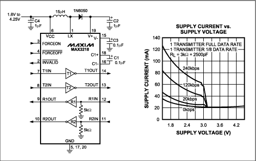
Figure 1. The MAX3218 employs a boost converter followed by a charge pump inverter, and its supply current rises with lower supply voltage. Why Not the Triple Charge-Pump Approach? A triple charge pump offers another straightforward approach to the RS-232 power supply (Figure 2). The first pump doubles the input voltage from + 2.5V to (theoretically) + 5V. But, ohmic losses in the charge pump and dropout in the transmitters prevent that voltage from achieving the ± 5V RS-232-compliant output levels. Another two charge pumps are therefore employed to generate the required + 5V and –5V transmitter-output voltages. 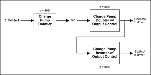
Figure 2. Because it is inefficient, the use of three charge pumps for generating RS-232-compliant transmitter-output voltages is not suitable for low-power RS-232 devices.
Though suitable for higher supply voltages, this topology is not suitable for low-power RS-232 devices operating from low voltages. The first disadvantage is poor efficiency. The input current is 42mA, assuming a required transmitter current of 5mA for a 120kbps data rate , a standard load of 3kΩ / 2500pF in parallel, and a typical charge-pump efficiency of 80% in each section. Though only a first-order estimation, that input current shows that the required power level (105mW) does not offer much improvement over a MAX3218.
A triple-charge-pump IC eliminates the switched DC-DC converter, but its chip size is large because the power MOSFETs (for charging and discharging capacitors in the third charge-pump section) require a lot of die area. A larger package and higher price would be the consequences. Moreover, the part would require two more external capacitors than does the double-charge-pump approach. For those reasons, Maxim takes another path in realizing low-voltage, low-power, serial interface devices.
Table 1. Electrical specifications for the EIA / TIA-562 serial-interface standard (compare with Table 1sb in Sidebar) Parameter Conditions Value Data Rate 1000pF capacitive load 60kbps Transmitter output range, minimum 3 ... 7k_ load, 0V offset, 0 level + 3.7V 3 ... 7k_ load, 0V offset, 1 level -3.7V Transmitter output range, maximum Open circuit, 0 level + 13.2V Open circuit, 1 level -13.2V Transmitter short circuit current, maximum 60mA 60mA
Maxim offers a variety of serial-interface ICs operating with supply voltages down to 2.25V. These devices target palmtop computers, handheld instruments, PDAs and cellphones. All are compatible with the RS-232 interface standard and compliant with EIA / TIA-562 ( transmitter output amplitudes are below 5V but above 3.7V). All operate with dual charge pumps. No DC-DC converters or triple charge pumps are necessary with this topology, so the result is much lower operating current. Other attributes of these devices include high ESD protection and small packages.
When designed with a MAX3316E transceiver, the 120kbpsec serial-interface circuit above draws only 15mA from a 2.5V supply. The resulting power consumption (37.5mW) is only 30% of that with a MAX3218 transceiver, even though the load (2500pF) represents a pretty long cable! Most portable devices are not connected to a PC with 15-meter cables, so a more reasonable assumption for cable length is two meters or less. The capacitive load for such cables is 500pF maximum, which further reduces the supply current to 8mA (Figure 3), resulting in power consumption of only 20mW. The rule is simple: short serial-data cables draw less current from the supply voltage. With short cables, the transmitter output voltage (well above + 4V and below –4V ) is in line with the EIA / TIA-562 specification and RS-232 compatible. 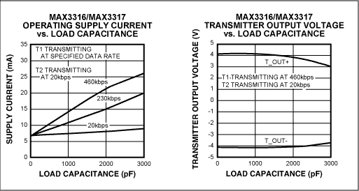
Figure 3. The MAX3316E draws low supply current from a 2.5V supply (left). Its transmitter-output voltages (right) are compatible with the RS-232 specification and compliant with the EIA / TIA-562 specification. Put All Electronics in the Portable Device, and Get Rid of the Active Cable! Personal digital assistants (PDAs) and high-end cellphones often exchange files with notebooks or desktop computers. The serial data link in these devices gets frequent use, so it makes sense to include the RS -232 transceiver in the portable device. Thus, signals with RS-232-compliant or -compatible voltage levels are available directly at the subminiature connector. Active circuitry is no longer needed within the cable connector, so that circuitry can be purely passive.
ESD protection on the logic side of the RS-232 transceiver is another advantage. A new package technology called chip-scale packaging (CSP) enables the smallest IC sizes possible, and allows integration into portables with very little board area. The size of such a package is not much greater than that of the die itself. It is bonded to the board by ball grids arranged in a matrix pattern. The MAX3228E is available in this new package, with a 5x6 ball grid matrix and 2.5x3mm dimensions. It therefore occupies an area of ​​only 7.5mm². Figure 4 includes the MAX3228E block diagram, its pin assignment, and a dimension drawing that shows how that IC fits into a portable device. Only four small 100nF capacitors are required to run the internal double-stage charge pump. 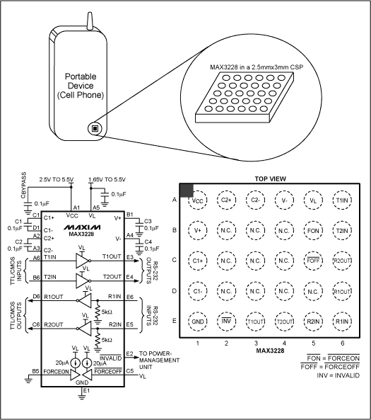
Figure 4. The MAX3228 includes two transmitters and two receivers. Available in a 5x6-grid chip-scale package (CSP), its small size allows easy use in portable devices.
In addition to the MAX3228E with its two transmitters and two receivers, the MAX3229E (available in the same UCSP package) includes one transmitter and one receiver. Both include AutoShutdown â„¢. Like the MAX3388E in the data-cable example, the MAX3228E includes a VL pin that can be operated down to 1.65V for low-voltage logic systems. Stay Compliant as Long as PossibleThe MAX3228E and MAX3229E (available in CSP) can be powered over a wide range of supply voltages (+ 2.5V to + 5.5V). To remain compliant with the RS-232 specifications (assuming VCC is high enough), the output-voltage swings for each device change from "compliant" to "compatible" when VCC falls below approximately + 3.1V. Details are shown in Table 2. The reduced output levels also extend battery life by reducing the supply current.
For the VCC input, a built-in hysteresis of about 400mV prevents output-level changes when VCC is noisy or subject to step changes in supply current. When VCC rises above approximately + 3.5V, the outputs return to RS-232-compliant levels . This feature allows the MAX3228E to be supplied from a single Li + cell. Thus, the MAX3228E provides fully compliant output-voltage swings while the battery is fully charged. As the battery discharges, at some point the device switches automatically to RS-232- compatible outputs, thereby ensuring operation of the serial port until the battery is fully discharged.
Table 2. Maxim transceivers automatically change to RS-232-compatible mode when their dual charge pump no longer provides RS-232-compliant output voltages.
Be Compatible, Not CompliantThe simple formula for saving power is to be compatible but not necessarily compliant with the RS-232 specification. To communicate over a short cable, it is not strictly necessary to comply with the 5V output-voltage amplitude, because the receiver input thresholds are specified at + 3V and –3V. A 2V drop is unlikely in a short RS-232 cable! That condition appears to violate the RS-232 specification in Table 1, but consider an electrical specification that was created in the early nineties to be fully compatible with the RS-232 specification. Transmitter Outputs Parameter Conditions Min Typ Max VCC Mode Switch Point (VCC Falling) T_OUT changes from ± 5V to ± 3.7V 2.85V 3.1V VCC Mode Switch Point (VCC Rising) T_OUT changes from ± 3.7V to ± 5V 3.3V 3.7V VCC Mode Switch Point Hysteresis 400mV Output Voltage Swing VCC = + 3.1V to + 5.5V,
VCC falling
VCC = + 2.5V to + 2.9V ± 5V ± 3.7V ± 5.4V
Called EIA / TIA-562, it was invented to support serial data communications at lower supply voltages, especially over short cables in quiet environments like offices, homes, and hotels. It targets communications between battery-operated portable devices and computers. You can compare major parameters in the EIA / TIA-562 specification of Table 1 with those in the RS-232 specification of Table 1sb in the sidebar. Neither spec defines a maximum cable length, but the EIA / TIA's maximum capacitive load (1000pF) implies shorter cables than does the RS-232's 2500pF.
The EIA / TIA maximum-specified data rate is higher (60kbps), but 120kbps and above are already used in many applications. The minimum transmitter-output amplitude (3.7V) is 1.3V below the RS-232 specification, and is compatible with quiet environments and a low voltage drop in the cable. Still, 3.7V leaves a headroom of 700mV with respect to the specified receiver thresholds of + 3V and –3V. Thus, an RS-232 receiver has no problem in understanding signals from an EIA / TIA-562 transmitter.
The maximum output amplitude is rated 13.2V, but (as discussed earlier) the target is to save power by operating the serial interface at the lowest possible voltage. In practice, actual receiver thresholds range below + 3V and above –3V. Though not specified , this fact provides another safety margin. The old quad-receiver MC1489 has typical high and low receiver-input thresholds of 1.3V and 1.0V. The corresponding MAX3225E thresholds are specified at 1.5V and 1.2V, as are those of other interface parts . Therefore, the assumption that most positive thresholds are below 2.0V and negative thresholds above 0V allows an additional voltage drop on the cable. Typical Data-Cable Application In a simple data-cable circuit (Figure 5) the interface driver is often placed within the housing of the subminiature connector that is plugged into the portable device. (For applications that require fewer receivers or transmitters, several other transceivers are available to replace the MAX3388E.) 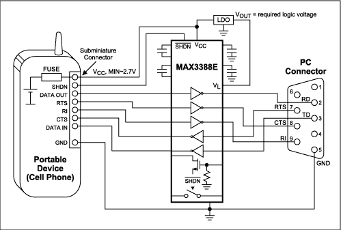
Figure 5. Data-cable designs are simplified by the MAX3388E's programmable logic voltage and a third transmitter, which is used to generate a ring-indicater (RI) signal.
The MAX3388E was chosen for this example because it offers advantages that help to resolve data-cable issues such as logic levels. The receiver outputs of an RS-232 interface device normally swing between 0V and VCC, which can be excessive if logic I / O in the portable device operates at voltages lower than VCC. The MAX3388E therefore provides a separate logic-supply input (VL) that sets the logic-high level for receiver outputs and the threshold voltages for transmitter inputs.
The VL pin works down to 1.8V, and allows flexibility in interfacing to most portable devices. Also simplifying the interface is an LDO (low-dropout linear regulator), whose output voltage can be set to the required logic-voltage swing. Or, you can save money by stabilizing the VL voltage with a zener diode or with diode drops (several 1N4148s in series). If VCC on the subminiature connector is constant (because an internal LDO is already stabilizing the output voltage) it might be sufficient to adjust the VL voltage with a resistor divider. Because VL supplies the receiver outputs, however, that solution depends on load capacitance at the receiver outputs and current flowing into the mobile device. A lowΩ resistor devider may be required to avoid larger voltage changes on the VL pin. More Features That Help Out.... A third transmitter in the MAX3388E can generate a ring indicator signal (RI) that alerts a UART in the PC or notebook. It can generate an interrupt whose associated sof tware routine can service full-duplex communications between the portable device and the computer. The MAX3388E contains a power switch for powering external circuitry such as the hot-sync circuitry in cradle applications. It is also equipped with a logic-level receiver between the RS -232 side and CMOS-logic side. Equipped with open-drain outputs, this logic-level receiver is also suitable for "hot syncing" and other dedicated communications.
All transmitters and receivers on the RS-232 side feature ESD protection to ± 15kV. (The logic side of the data cable may need additional ESD protection not shown in Figure 6.) For MAX3238E and MAX3248E RS-232 transceivers, both the logic and RS-232 sides are ESD-protected. Those devices remain RS-232 compliant down to VCC = + 3.0V, and RS-232-compatible down to VCC = + 2.7V. Small-Footprint, Lowest-Power, RS-232- Compatible Parts Run on + 5VDigital still cameras, point-of-sale systems, and set-top boxes often include an RS-232 serial interface and run from a single + 5V supply. Those applications get along with short data cables, so the EIA / TIA-562 standard is fully sufficient. Other transceivers are designed around the MAX3311E for just those kinds of applications. The + 5V-only parts work with a single charge pump that reduces the number of external capacitors, and their µMAX packages occupy very little board space. These parts also offer RS-232-compatible transmitter-output swings. The MAX3311E is probably the lowest-power serial interface available: with a 120kbps data rate and a short cable exhibiting less than 500pF of capacitance, it requires an operating supply current no higher than 2.5mA!
Sidebar RS-232 Transceivers: Historical Development of the Modern ICEarly versions of the RS-232 interface consumed lots of power! More than 20 years ago, a serial interface was normally built with the standard devices then available: the quad-transmitter MC1488 and quad -receiver MC1489. Then and today, those devices were available from National Semiconductor, Texas Instruments, On Semiconductor, and others. Because they were manufactured with a bipolar silicon process, they had very high quiescent currents.
In those days, an MC1488 / MC1489 pair dissipated more than 700mW! And when transmitting data, the pair's additional driver currents and cable-charging losses boosted power dissipation as high as 1W. For years, a big disadvantage of the transmitter device was the requirement that power-supply voltages be symmetrical around ± 12V (approximately). Receivers operated from a single + 5V supply, so an RS-232 port required three supply voltages. The situation was worse for desktop computers, whose two COM interfaces were usually implemented with the standard SN75185 driver, which includes three transmitters and five receivers. Power dissipation was 1.2W, even when the interface was not in use. The RS-232 SpecificationA designer was lucky if his system already included analog circuitry (such as op amps) operating from ± 15V, from which the RS-232 supply voltages could be derived. On the other hand, the necessary serial-interface supply voltages had to be generated from digital systems that opera ted from + 5V alone. After all, the RS-232 specification requires voltage amplitudes at the transmitter outputs to be at least 5V (Table 1sb).
Note that outputs of the RS-232 standard are inverted: sending a logic-high signal on the TTL side produces a negative voltage on the RS-232 side equal to or less than –5V, and sending a logic-low signal produces a positive voltage equal to or greater than + 5V. The receiver threshold is specified at ± 3V, which allows headroom for data transmission over long cables and increases the immunity against distortion.
Table 1sb. Selected Electrical Specifications from the RS-232 Serial-Interface Standard. Parameter Conditions Value Data Rate 2500pF capacitive load 20kbps Mode of operation Single-ended Allowed # of Tx and Rx per data line Per line 1 Tx, 1 Rx Cable length, maximum Load dependant Transmitter output range, minimum 3-7kΩ load, 0V offset, 0 level + 5V 3-7kΩ load, 0V offset, 1 level -5V Transmitter output range, maximum Open circuit, 0 level + 25V Open circuit, 1 level -25V Transmitter short circuit current, maximum 100mA Receiver input resistance 3kΩ to 7kΩ Instantaneous slew rate 6V / µs <Sr <30V / µs Receiver input sensitivity, high + 3V Receiver input sensitivity, low -3V Receiver input range, maximum High + 25V Low -25V
Many people still believe that the RS-232 transmitter must be supplied with ± 12V. Those levels were an unofficial standard for many years, because often they were already available for analog circuitry or for the hard-disk drives in computers. The ± 12V rails were convenient but not strictly necessary, as Table 1sb illustrates.
It is sufficient to provide just enough output voltage. An RS-232 interface is fully compliant with its specification if the output reaches the required minimum amplitude of 5V, so a ± 6V supply might be adequate for transmitters with very little voltage drop across the output stage. On the other hand, ± 12V rails may offer the advantage of additional noise immunity for data transmission over long cables in an industrial environment.
Most of today's RS-232 communications, however, require cables of less than three meters, eg, connecting a cell phone or PDA cradle to a notebook computer, or a small PBX to a desktop PC. Those applications reside in the office or in the home, so noise immunity is not a big issue. Note that the RS-232 standard specifies a maximum load capacitance (2500pF) rather than a maximum cable length. Thus, even for cheap interface cable exhibiting a capacitance of 100pF / m, cable lengths up to 25 meters should pose no problem. First Challenge: Get Rid of the Big Power Supply! When Maxim announced the MAX232 transceiver in the mid-1980s, no one knew how successful it would become. Today it is offered by more than 10 manufacturers , with a volume of several million per year. Its main feature is + 5V single-supply capability, so the symmetrical bipolar supply voltages are no longer needed. Nevertheless, its outputs offer signals compliant with the RS-232 specification.
The simple idea behind this IC design was to integrate the charge pumps. Figure 1sb shows the internal charge pump, which doubles the input voltage in a first stage and then inverts it in a second stage. That way, it derives from + 5V inputs a doubled voltage of + 10V (theoretically), and then an inverted voltage of –10V (also theoretically). Actually, ohmic and switching losses reduce the typical MAX232 output swings to about ± 8V. Today, the MAX232 circuit is basic to more than 100 RS-232 devices offered by Maxim. 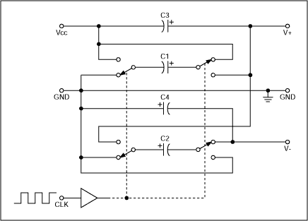
Figure 1sb. Transmitter output stages in a MAX232-type RS-232 transceiver derive their positive and negative levels from the V + and V- voltages produced by internal charge pumps. The Next Challenge: A + 3.3V Single SupplyWith logic-supply voltages decreasing to 3.3V, the convenient solution of a double-stage charge pump suddenly became obsolete. The MAX232 won't operate at + 3.3V and is not specified at that level. Theoretically, doubling and inverting that low voltage with charge pumps would produce symmetrical rails of ± 6.6V, but losses in the internal charge-pump transistors and transmitter-output stages are too high to provide output amplitudes compliant with the specifications listed in Table 1sb. Note also, that a + 3.3V supply specified with high tolerance (± 10%) provides a minimum rail of only + 3.0V.
Maxim designed the next generation of parts accordingly, and those parts are available from other manufacturers as well. Nearly all such ICs feature low supply current and ± 15kV ESD protection according to the IEC1000-4-2 standard. The new devices have high-performance charge pumps with very low loss in the switching transistors, and their transmitter-output stages feature low dropout voltage. As a result, the members of this family operate with supply voltages down to + 3.0V. The MAX3225E, for instance, containing two transmitters and two receivers, is functionally similar to the good old MAX232. But, the ICs of this family feature new capabilities that make the designer's job much easier.
Supply voltage range is + 3.0V to + 5.5V, allowing the part to be used in either + 3.3V or + 5V systems. For most applications, a large manufacturers need qualify only one standard RS-232 part.
Regulated charge pumps save transmitter current. A small but effective trick for saving power is to limit the transmitter output voltage. Unfortunately, designers have no influence on the resistor that terminates the driver output, which is specified at 3kΩ to 7kΩ. Data sheets are normally specified with maximum load on the transmitter, which occurs at 3kΩ. Power dissipation in the termation resistor is PDIS = V² / RTERM. Thus, it makes sense to limit the output voltage, which appears in this equation with a power of two!
Maxim's low-voltage RS-232 devices feature output-voltage control. Note that higher supply voltage allows less switching activity in the charge pumps. The internal charge pumps generate ± 6V by pulse control, independently of the supply voltage. The low-dropout transmitter -output stages then deliver voltages of ± 5.5V, which are nevertheless compliant with the RS-232 specification. These stages provide an impressive invariance of output voltage with load capacitance, even at data rates above 1Mbit / s (Figure 2sb). The MAX232 with its 8V output amplitude dissipates 21.3mW in the termination resistor, and output-voltage control drops that power dissipation to 10mW, a power saving of more than 50%! 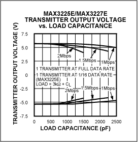
Figure 2sb. MAX3225E transmitter outputs remain compliant with the RS-232 specification, even with a 1Mbit / s data rate and 2000pF load capacitance. Switch it Off! The power-saving shutdown modes AutoShutdown ™ and AutoShutdownPlus ™ operate without the help of software. AutoShutdown, for instance, is voltage-triggered. The part switches off when more than 30µs elapses with no valid voltage levels at the RS-232 inputs, as normally occurs when the cable is unconnected or the transmitters on the opposite side are switched off. As soon as a valid voltage appears at one of the receivers, the part wakes up and is immediately ready for operation.
This shutdown mode has two caveats: First, the part does not shut down as long as a valid voltage is present at one of its RS-232 receiver inputs. That can be a problem when a transmit voltage on the other side is not properly switched offæthe result can be a continuous valid signal that prevents the part from going into its current-save mode. Second, the part needs to be awakened before sending data.
AutoShutdownPlus fixes the disadvantages of AutoShutdown. It monitors receiver inputs on the RS-232 side and transmitter inputs on the TTL side as well. Its edge-triggered operation poses no problem with continuous signals. The part goes into shutdown mode when more than 30 seconds pass with no receive or transmit activity. Then, an edge at either the RS-232 inputs or the transmitter's TTL-side inputs causes the part to wake up.
A similar version of this article appeared in the July 2002 issue of Portable Design magazine.
Lower the Supply Current in Yo
Abstract: When considering an integrated circuit, today's design engineers look for low-power features as well as performance. Saving a few milliamps of quiescent current per chip may seem trivial, but it becomes substanTIal for a board with dozens of ICs. Such savings allow the use of smaller Power Supplies and less power drawn from the wall outlet. For small, portable, battery-operated devices, power savings allow longer operaTIon from the battery.