Guide: When it comes to the challenging issue of switching power supplies, PCB layout is not particularly difficult. However, if you aim to design a high-quality PCB board, it becomes one of the most challenging aspects of switching power supply design (poor PCB design can lead to situations where no matter how you adjust the parameters, the debugging process fails). This is not an exaggeration. The reason is that there are many factors to consider during PCB layout planning, such as electrical performance, manufacturing process, safety requirements, and EMC impact. While basics are important, EMC is the most complex to understand, and the bottleneck for many projects often lies in EMC issues. Below, I will share 22 key points on PCB layout and EMC.
First, understanding the circuit makes PCB design and EMI circuit design easier
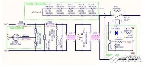
The influence of the above circuit on EMC can be imagined. There's a filter at the input, pressure-sensitive components for lightning protection, resistor R102 to prevent inrush current (to reduce losses with the relay), the key differential mode X capacitor and the matched inductor with the filtered Y capacitor, and also a fuse that affects layout. Each component here is critical, and the function of each device must be carefully evaluated. The level of EMC severity to be considered when designing the circuit should be designed with ease, such as setting multiple levels of filtering, the number of Y capacitors, and their placement. The choice of pressure-sensitive size is closely related to our demand for EMC. Welcome to discuss how seemingly simple EMI circuits contain profound principles in each component. Second, the relationship between the circuit and EMC: (taking the most familiar flyback main topology as an example, see which key parts of the circuit contain the mechanism of EMC)
The circuit in the above figure has several loops, which are very important for EMC (note that the green part is not). For instance, everyone knows that electromagnetic field radiation is spatial, but the basic principle is the change in magnetic flux, and magnetic flux relates to the effective cross-sectional area of the magnetic field. That is, the corresponding loop in the circuit. Current generates a magnetic field, producing a stable magnetic field that cannot convert into an electric field; however, changing current produces a changing magnetic field, which can generate an electric field (this is essentially Maxwell’s equation explained in simple terms). A changing electric field can similarly generate a magnetic field. Therefore, we need to pay attention to places with switch states, which are one of the sources of EMC. Here, one of the EMC sources is shown (others will be discussed later). For example, the dotted loop in the circuit, the loop when the switch is turned off. Not only does the switching speed affect EMC when designing the circuit, but the layout routing area also plays a significant role! The other two loops are the absorption loop and the rectification loop. We'll go into more detail later!
Third, the relationship between PCB design and EMC 1. The impact of the PCB loop on EMC is very important. For example, the flyback main power loop, if too large, leads to poor radiation. 2. Filter routing effect: the filter is used to eliminate interference, but if the PCB trace is not well-designed, the filter may lose its effectiveness. 3. Structural part: grounding of the heat sink design affects the grounding of the shielding plate, etc. 4. Sensitive parts being too close to the interference source. For example, the EMI circuit and the switch tube being too close can inevitably lead to poor EMC, requiring clear isolation areas. 5. RC absorption loop routing. 6. Y capacitor grounding and routing, and the location of the Y capacitor is also very important! And many more. I’ll think of this first and say this, and then we’ll discuss in detail, starting with an introduction. Here’s a small example:
As shown by the dotted line in the above figure, the X capacitor pin routing has been retracted. You can learn how to make the capacitor pin wire plug-in (using a squeezed current trace). In this way, the filtering effect of the X capacitor can be optimally achieved. Fourth, PCB design preparation: (preparing enough allows for step-by-step design, avoiding design reversal) There are some aspects listed below, which are based on my own design process. All content is unrelated to other tutorials, just a summary of my own experience. 1. Appearance structure size, including positioning holes, airflow direction, input and output sockets, matching with the customer system, and communication with the customer about assembly problems, height limits, etc. 2. Safety certification, what kind of certification is required for the product, where the basic insulation creepage distance needs to be sufficient, and where to strengthen insulation to keep enough distance or slots. 3. Package design: no special periods, such as custom package preparation. 4. Process route selection: single panel vs double panel selection, or multi-layer board, based on the schematic and board size, cost, and other comprehensive evaluation. 5. Other special requirements from the customer. The structural process is relatively flexible, while safety regulations are relatively fixed. What certifications are used, what safety standards have been passed, and of course, some safety regulations are common across many standards, but some products like medical devices are more demanding. For new engineers, friends won’t be overwhelmed. Next, I’ll list some general products commonly used, and the following is the specific layout requirements for IEC60065, for safety regulations, we need to remember them, and when encountering specific products, we need to target them: 1. The distance of the input fuse pad parts is greater than 3.0MM, and the actual layout is 3.5MM (simply say 3.5mm creepage distance before the fuse, then 3.0mm creepage distance) 2. Before and after the rectifier bridge safety requirements 2.0 MM, the layout is in accordance with 2.5MM. 3. After rectification, the safety regulations are generally not required, but the high and low voltages are kept at a distance according to the actual voltage. It is customary to use 400V high voltage to stay above 2.0MM. 4. The safety requirements between the primary and secondary are 6.4MM (interval), and the creepage distance is best according to 7.6MM. (Note that this is related to the actual input voltage. It is necessary to check the specific calculation of the table. The data is provided for reference only, subject to the actual situation.) 5. The primary and secondary use cold ground, hot and clear identification; L, N logo, input AC INPUT logo, Fuse warning signs and so on need to be clearly marked.
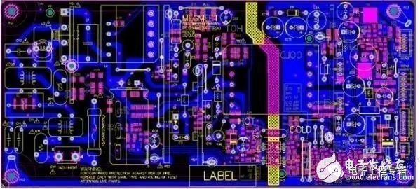
If you have questions about the above, you can also discuss and learn from each other! Reaffirm that the actual safety distance is related to the actual input voltage and the working environment. It is necessary to check the specific calculations. The data is provided for reference only, which is subject to the actual situation. 5. The safety of the PCB design considers other factors . 1. Understand your own products. What kind of certification, what kind of product, such as medical, communication, electricity, TV, etc. are different, but there are many similar places. 2. Where the safety regulations are closely related to the PCB layout, understand the characteristics of the insulation, which areas are basic insulation, and which places are reinforced insulation. The insulation distance of different standards is not the same. It is best to check the standard and calculate the electrical distance and creepage distance. 3. The safety device of the product pays attention to, such as the relationship between the magnetic properties of the transformer and the original secondary side. 4. The distance between the heat sink and the surrounding area is different. The grounding of the radiator is not the same. The grounding is still cold, and the ground is insulated. Also clothed. 5. The insurance distance is especially noticeable and requires the strictest places. The distance between the front and rear of the fuse is the same. 6.Y capacitance and leakage current, contact current relationship. The follow-up will explain in detail how to stay and how to do the safety requirements. Sixth, PCB design power layout 1. First measure the PCB size and the number of devices, to achieve sparse and dense, or a piece of dense, a piece of sparse is difficult to see. 2. The circuit is modularized, centered on the core device, and the key device is placed first. 3. The device is placed vertically or horizontally, one is beautiful, the other is to facilitate the operation of the plug-in, and the tilt can be considered in special cases. 4. The layout needs to take into account the routing, and put it in the most reasonable position to facilitate subsequent routing. 5. Reduce the loop area as much as possible during the layout. The four major loops will be explained in detail later. To achieve the above points, of course, to be flexible, a more reasonable layout will soon be born. The following is the first virgin PCB board I drew. Many years ago, it was very difficult to accomplish at the time. There may be minor problems in the middle, but the general layout is worth learning:
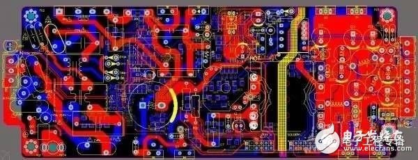
The power density of this figure is still relatively high. The control part of the LLC, the auxiliary source part and the BUCK circuit drive (high power multi-output) are not on the small board. Look at the layout characteristics of the main power: 1 The input and output terminals are fixed dead, can not move, the board is rectangular, how to choose the main power flow? Here, it is laid down from the bottom to the top, and the heat is relied on the outer casing. 2. The EMI circuit is still in a clear flow direction. This is very important. If it is not confusing, it is not good for EMC. 3. The position of the large capacitor considers the PFC loop and the LLC main power loop as much as possible. 4. The current of the secondary side is relatively large. In order to take the current and heat dissipation of the rectifier, the layout is adopted, the rectifier is on, and the BUCK circuit is used. The MOS tube is under, the heat dissipation effect is good; the top layer of high power is generally negative, and the bottom layer is positive. Each board has its own characteristics, and of course it has its own difficulties. How to solve it properly is the key. Can you understand the meaning of reasonable layout selection? Seven, PCB instance appreciation can be based on the PCB layout points discussed before, check this board, whether it is done in place, I think it is a better place, of course, there will always be, you can also come up, single panel is so compact It is not easy to do this, you can learn from this board! Later, I will explain the learning for this board. Let's enjoy it first.
Eight, PCB design of the four major loops: (the basic requirement of PCB layout is that the four major loop areas are small)
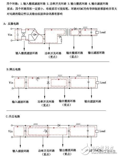
In addition, the absorption loop (RCD absorption and RC absorption of the MOS tube, RC absorption of the rectifier) ​​is also very important, and it is also a loop for generating high-frequency radiation. Any doubt about the above figure is welcome, and there is no fear of any doubt. As long as it is a questioning of the problem, it is a better progress to discuss and study together! Nine, PCB design hotspots (floating potential points) and ground lines:
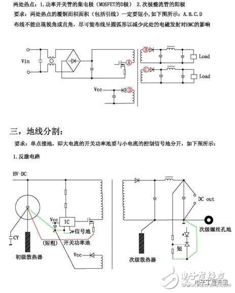
Matters needing attention: 1. For hotspots, we must pay special attention to (high-frequency switching points), which is a high-frequency radiation point. The layout of the wiring has a great influence on EMC. 2. The loop formed by the hot spot is small, the trace is short, and the trace is not as thick as possible, but enough to take enough current. 3. Ground wire should be grounded at a single point. The main power ground is separated from the signal ground, and the sampling ground is separated. 4. The ground of the radiator needs to be connected to the main power ground. Ten, EMC rectification experiences are personal understanding, there may be differences between traditional information materials, at your own discretion, anyway, I think many common materials results did not use my own summary, boast of. I want to say a lot, it may be a little messy, it is practiced! How to understand the results of EMC production and testing: simply speaking, how to prescribe the right medicine, many cases get the first round of test results, how to get results and power To control analysis; the main ideas are as follows: 1, for conduction, the test range standard 15K-30M, the common EN55022 is 150K. How did the source of conduction come about? For the low frequency, mainly the switching frequency and its multiplier (followed by the diagram), this source can not be solved, the switching frequency can not be eliminated, of course you can change the switching frequency, it just moves the test results, and There is no real sense of elimination. Can only be solved by the filter, generally for the low frequency R10K high magnetic flux material has a good effect, the size of the magnetic ring is related to your power, generally up to 10MH sense, even larger to 20MH, with Y Capacitance can generally be solved very well, low frequency is not difficult; the real difficulty is high frequency, personally think that the cause of high frequency is much more complicated, there are switches, there are transformers, there is also the possibility of inductance, that is, everything exists in the switch state The place may exist (how to judge the specific location, follow-up explanation), here need to find some way; find the source may not be able to solve the source, there may be improvement, or the matching filter. For high frequency, low magnetic flux material, such as nickel-zinc ring, the sensitivity is generally UH level, with the appropriate Y capacitor (more complicated power supply, it is recommended to leave a few Y capacitor position when laying the board, easy to rectify); 2 Some cooperation methods, many textbooks have mentioned increasing the X capacitance to judge the differential mode or the common mode. There is a certain meaning that the actual help is not great. Generally, our X capacitors will be put into appropriate values ​​during design. And increasing the X capacitor can solve the differential mode problem, but it is also awkward, so many textbooks provide a certain meaning guidance, personally feel that it is useless. I think there are several better means: 1. Summarize the differences against grounding and incomprehensibility. Ungrounding may be worse, because the system has less conduction paths; it may also be improved, indicating that it is conducted to the port through the ground loop. . Specific solutions, adjust the point Y capacitance of the circuit ground and add magnetic beads. 2. Set the magnetic ring on the input port. If the low U ring is improved, adjust the first stage filter inductor. 3 complex systems pay attention to the shielding measures of EMI circuits. If the measures have no effect, reflect on the PCB design, this aspect will be mentioned in the PCB design. 3, for radiation: must find the source to solve, observe the first test results, if it is beyond 30M, related to grounding, the system to find the ground, and to determine whether the test is well grounded, sometimes the input line has an impact. Within 2.40M-100M, it is usually caused by the turn-off of the MOS tube. Sometimes it is judged whether it is turned on or off for the sake of the site. It can be verified by correcting the observation results (of course, this will cost money, and the follow-up will explain how to use The oscilloscope judges, this is a secret trick). 3 100M or more is mostly caused by diodes, rectify the diode absorption capacitance, and some of the high power may be synchronous rectification, change the MOS tube absorption loop, remember that sometimes it is necessary to adjust R with R. To say too much, follow-up to specific examples to add it, first hand to play so much, anyway, I played hard enough, can cause resonance is difficult, after all, everyone's rectification experience is much worse, just give some new friends a revelation, Follow-up examples! XI. Layout of the filter wire The filter line of the filter capacitor has a vital effect on the filtering effect. If it is not good, it may lose its proper filtering effect. Figure 1 shows the secondary side rectification and filtering method to spread the effect of the two capacitors to avoid the failure of the second capacitor in the rectifier circuit.
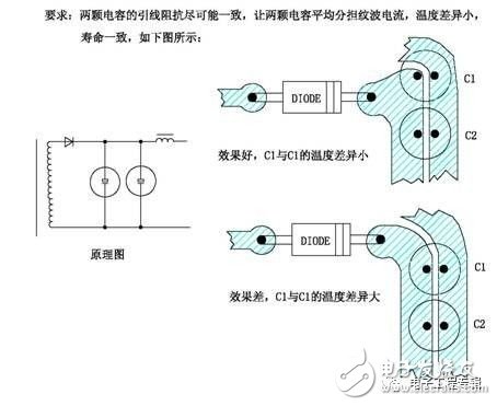
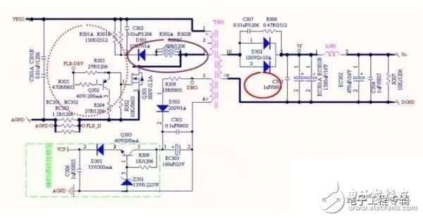
Figure 2: For the output filter capacitor trace, it must not be plugged (that is, bypassed), and the output ripple is not good.
Twelve, the layout of the LLC circuit and EMC
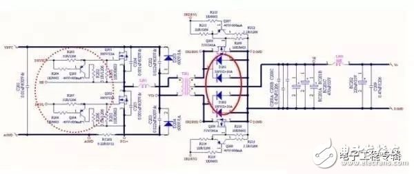
The LLC circuit is the most familiar to everyone. The dotted circle is the driving circuit. When the circuit is designed, it is placed close to the MOS tube. That is to say, the driver provided by the IC only needs to draw two wires to the driving circuit. The driving circuit is close to the MOS tube to avoid Be disturbed (at the same time, when driving the line, pay attention to the drive to the sensitive signal, which is both the sensitive signal and the interference source); once the drive is disturbed, the power supply can be imagined. Similarly, the MOS tube drive of the synchronous rectification should also be close to the synchronous rectifier. The design schematic diagram can be well understood as shown in this figure. If you give this circuit to the PCB engineer, he is very intuitive how to layout the trace. If you paint very messy, many PCB engineers may have a good understanding of the circuit and it may be easy to make a mistake. In addition: the primary side has an important loop, the PFC capacitor and the MOS tube and the transformer, the resonant inductor, and the resonant capacitor form a small loop area; the secondary side rectification and filtering loop is equally important, the capacitor has been said before the trace, and it is also very Important; Pay attention to the high and low voltage distance when routing. In some places, the voltage is floating and must be treated as high voltage, such as the upper tube drive and the corresponding reference voltage. As for the opening of the LLC aspect of the LLC, the soft switch has almost no effect on the EMC. The focus is on the speed of the shutdown speed on the EMC. The capacitance of the MOS junction capacitor has a great influence on the EMC. The capacitor is not suitable, or Is not added (MOS tube itself also has junction capacitance) may have an impact on EMC, this is the focus of attention; this figure does not have Y capacitor, the positive or negative anti-set Y capacitor in MOS tube can also filter the switch interference well; Any questions about this circuit can be discussed and grow up in the discussion! Thirteen, circuit design and layout of PFC
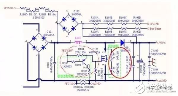
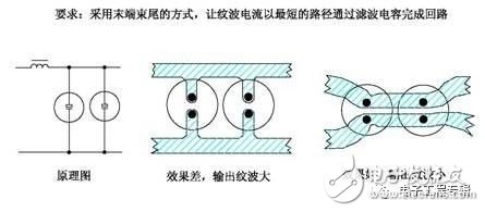
The above picture is a typical BOOST PFC circuit: The green box on the left is the drive circuit. Just like the previous LLC topology drive, it is placed close to the MOS, which is reflected on the schematic. The green dotted box on the right is the MOS tube turn-off spike absorbing circuit, which is the smallest loop with the MOS tube. The other two important loops are the MOS tube turn-on loop (dashed red graph) and the other MOS. pipe shutdown loop (solid red line chart); loop area as small as possible; XIV, magical ring in EMC EMC difficult to source some products up treatment, magnetic filter can be used, of course, I say here The magnetic ring has two levels of meaning. On the one hand, the filter inductance of the input and output ends, the magnetic ring of different materials is used, different numbers of turns have corresponding effects, and on the other hand, the magnetic ring is directly placed on the input and output lines. Sometimes it works, but it can't be used in all situations, at least it can be used as a basis for judgment;
The blue and black lines above are the positive and negative ends of the output, and a magnetic ring is placed on the top to solve the high-frequency end of the output rectifier. In some cases, the interference of the port on the PCB does not necessarily have an effect. The magnetic release ring on the line has an unexpected effect. Fifteen, the key signal of PCB routing
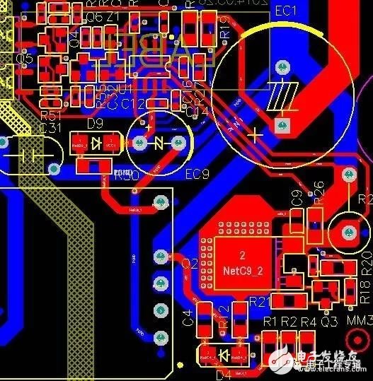
Note: 1. CS signal (sampling signal): Pull out from the sampling resistors R25 and R26. Note that the ground of the IC is based on the sampling resistor. The positive and negative differential traces of the sampling resistor pull down the IC CS pin and the GND pin of the IC. 2. The drive signal pulls down the IC drive pin from the drive circuit, taking care not to interfere with the CS pin; as shown in the figure, the three wires are routed side by side, and the ground wire is driven in the middle of the drive and the CS line to play a certain shielding role; The panel is best shielded from the ground layer of the IC. The network of the grounding must be drawn from the IC GND. The non-critical signal GND can be directly punched through the hole. The key signal ground needs a single point grounding and is directly connected to the IC. 4. FB feedback network signal Pay attention to check the trace and connect the IC at a single point; 5. Do not put the RCD absorption network in the main loop; 6. The rectification and filtering ground of VCC needs to be connected to the main power ground, and the secondary filter can be connected to the IC ground; 7. The Y capacitor wiring is connected separately. , can not be confused with the main power, to avoid interference; 16, the main power and control part of the wiring diagram
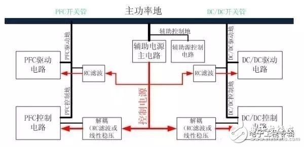
Many people may see this picture, in the cloud, generally introduced: 1. PFC drive and IC connected to the PFC tube, more specific point is the ground of the sampling resistor; 2. DC-DC part of the drive ground And control ground connected to the sampling area of ​​the DC switch tube; 3. The auxiliary source part is controlled to be connected to the auxiliary source MOS tube sampling, and the MOS tube ground is connected to the main power ground; 4. The power supply ground of each IC passes the auxiliary source EC filter IC Ground, pay attention to the RC filter close to the IC; Summary: pay attention to their respective single point grounding, the ground line is not chaotic, is one of the most important places of the line! ! ! XVII electromagnetic shielding mechanism analysis Figure 1: The principle of magnetic shielding
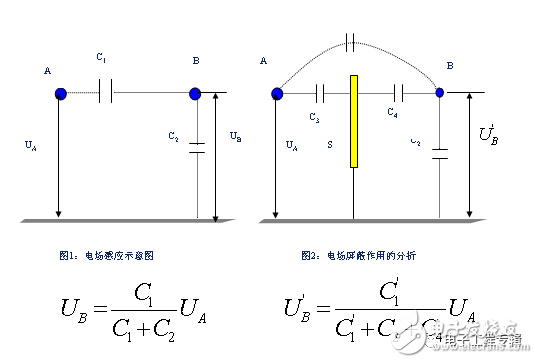
As shown in the figure: the electric field interference of the input and output can be coupled through the capacitor. If the shielding plate is added, the size of C4 is increased, and C1 is also reduced, which attenuates the electric field interference. Figure 2: Principle of magnetic field shielding
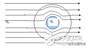
As shown in the figure: the characteristics of the magnetic field shielding are different from the magnetic field. The outer casing is shielded. The electric field only needs the plane shielding plate. Therefore, the shielding of the radiator brings the electric field shielding. Some closed-type power supply with the outer casing plays a certain magnetic field shielding. Principle, the magnetic field through the shield will change the magnetic circuit, causing the magnetic field to spread to the surrounding, the intermediate magnetic field interference to achieve the purpose of shielding; 18, the switching device and EMC understanding of the device also has important significance for EMC, such as MOS tube, main switch MOS It is one of the important EMC sources. The opening and closing of the rectifier also generates high-frequency radiation (the principle is that the current generates a magnetic field, and the changing current generates an electric field). Of course, the semiconductor switching device and other inductors are mainly introduced here. The transformer will not be explained; what parameters of the switching device have an important impact on EMC, we often say that the fast tube, the slow tube is what is the reference? We all know that the fast-opening loss is small, and we like to use it for high efficiency. However, in order to pass the EMC smoothly, we have to abandon the efficiency and reduce the switching speed to reduce the switching radiation. For the MOS transistor, the turn-on speed is driven by the driving resistor and the input junction capacitor. Determined; the turn-off speed is determined by the output junction capacitance and the internal resistance of the tube;
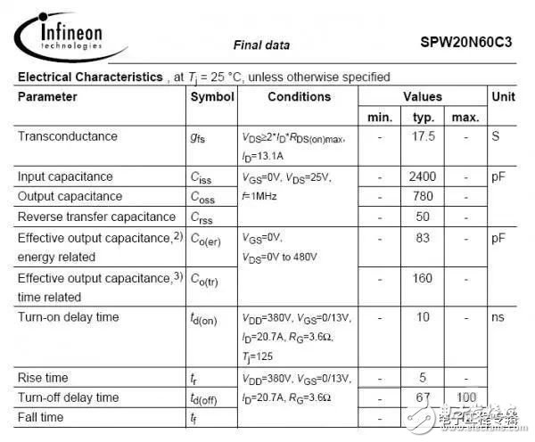
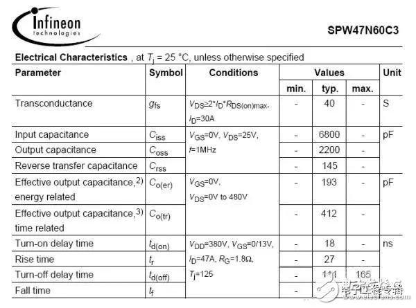
Referring to the above two figures, different types of MOS tubes, compared to the input junction capacitance and output junction capacitance, 2400PF and 800PF; 780PF and 2200PF; at first glance, the first specification is the fast tube, the second is the slow tube, this It is decided that the switching speed should be matched with the driving resistance. In general, the driving resistance is more in the 10R-150R. The driving resistance is related to the junction capacitance. The driving resistance of the Allegro can be appropriately increased, and the slow tube driving resistance can be appropriately reduced. There are Schottky diodes, fast recovery diodes, common diodes, and a relatively small number of SIC diodes. The switching speed SIC diode is almost zero, which is equivalent to no reverse recovery, minimum switching radiation, and minimal loss. The disadvantage is that it is expensive, so it is rarely used; the second is Schottky diode, the forward voltage is reduced, the reverse recovery time is short, followed by fast recovery and common diode; need to compromise between loss and EMC; generally can be taken Re-absorption and set of magnetic beads and other measures to rectify EMC; 19, EMC filter
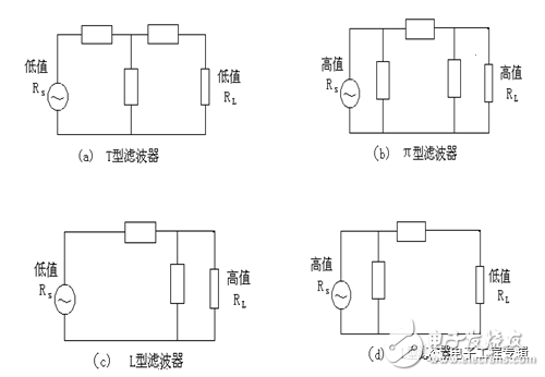
The choice of filter architecture is very important to the filter. In different occasions, the filter is filtered according to the impedance matching. You can choose how to filter according to the principle of this figure; for example, the most commonly used output rectifier bridge adopts π Type filtering and LC filter at the output;
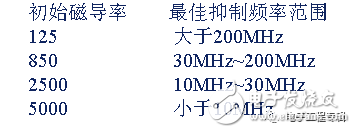
The material of the filter is also very important for designing the filter inductor. Materials with different initial permeability will work in different frequency bands. The wrong material will completely lose its proper effect. 20. EMC's flyback high frequency, etc. Effective model analysis
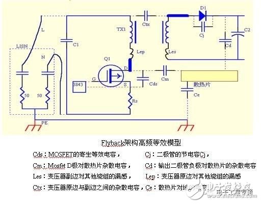
First understand the EMC: EMC path from the simplest model. Of course, space radiation is related to the loop, and the loop is also constructed by the path. The flyback high-frequency equivalent model is analyzed to help understand the mechanism of EMC formation. Our test The receiving device will receive conduction from the L and N terminals. In order to reduce the received interference, the interference must flow through the ground loop without flowing from the L, N port to the receiving device; at this time, our EMI inductor and Y capacitor pass impedance matching. Can be realized; in addition, the primary side interference can be formed by the primary secondary side Y capacitor, the transformer stray capacitance and the ground coupling to the secondary side to form more loops; of course, some junction capacitance parameters, such as MOS tube junction capacitance, heat sink junction capacitance Can constitute a circulation path; twenty-one, the form of radiation and frequency distribution
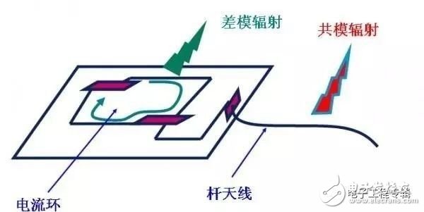
This picture may be somewhat abstract, but just as EMC is difficult to be specific, we need to give us some inspiration. It can be seen that the differential mode radiation exists in the form of a loop, and the common mode radiation is emitted in the form of an antenna; therefore, it just confirms In the front, when we lay out the layout of the switch loop and do not take the acute angle when laying the line, the conventional walk is 45 degrees, preferably the arc trace, of course, the trace efficiency will be relatively low; the basic knowledge of these principles is well understood. It is useful for actually handling EMC work and layout. If you don't have this kind of awareness, it may be useless. Because you can't provide a direct method, you need to combine it with other knowledge. And many of the principles mentioned here are in many EMC materials. Can't see it, and it's not so concentrated, you need to repeat it!
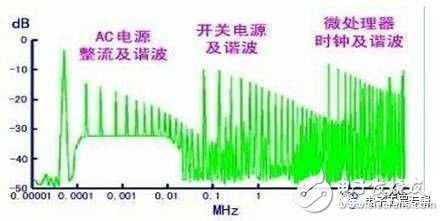
Figure: The relationship between some frequency ends and the location of the switching power supply. This is just a general rule. Don't believe it completely. Is it a law and can't believe it? Why? The law is not established in all situations, the difference between different power sources is also great, so the principle is to help you analyze, rather than follow the method to hard set; 22, EMC instance
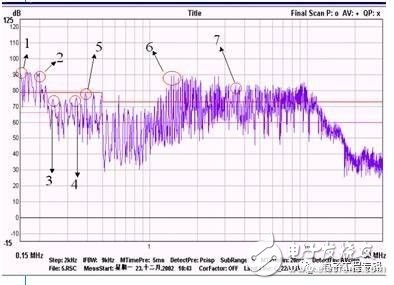
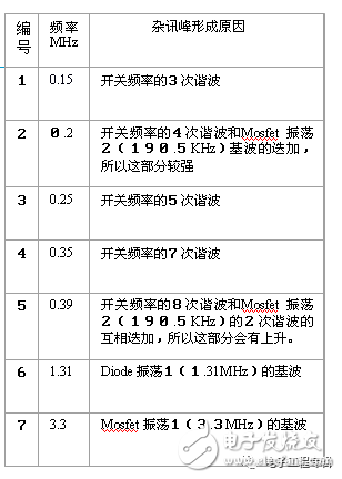
According to the conduction example, the key point of the frequency distribution point is the relationship between the specific data and the fundamental frequency. After this test, it is necessary to speculate on the laws of these values, and it may be possible to find any clues; of course, how these frequencies are solved by filters The means has also been said before; here is to add some seemingly mysterious EMC how it came from, it feels no longer mysterious, not just a confused filter to solve the problem!
This article is reproduced from the network, please contact us if you are interested in copyright.
Long press the QR code to identify attention

Oblique Single Axis Solar Tracker System
Oblique Single Axis Solar Tracker System,Oblique Single Axis Solar Tracker System Customized,oblique single axis solar tracker system device
Hebei Jinbiao Construction Materials Tech Corp., Ltd. , https://www.pvcarportsystem.com