Overview The DS1870 is used to bias RF power amplifiers. This application note illustrates how to use its two-dimensional lookup table.
Input to output path Figure 1 shows the path to detect the input to the output setting of the potentiometer tap position.
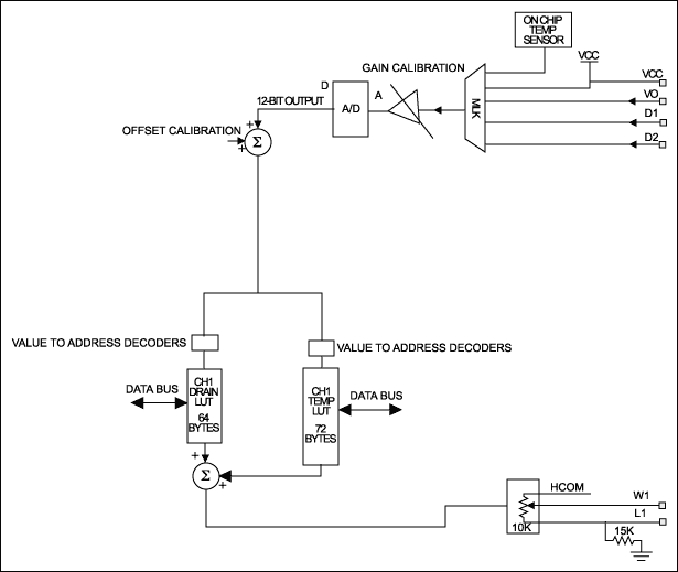
figure 1.
All inputs are single-ended inputs referenced to ground. In this example, the two very important signals are: ID1 and the on-chip temperature sensor. These analog signals are sent to the analog terminal of the A / D converter (ADC) through a multiplexer. Program the gain stage. After the ADC quantization, the offset calibration is applied to the digital part of the ADC. The gain and offset calibration (scaling ratio) can be programmed through the following calibration process. Each signal has its own gain and offset proportional coefficient. The values ​​obtained so far can be used as index pointers for two-dimensional lookup tables, one table is indexed by temperature value, and the other table is indexed by ID1. As the pointer moves from one position to another, the contents of the corresponding register are sent to the accumulator through the bus. The accumulator sums the values ​​of the two registers at the change time corresponding to the temperature and ID1. The summation result indicates the position of the center tap of the potentiometer.
Note: ID1 can be any voltage signal, which can represent current, external temperature or any other variable.
During proportional adjustment and calibration, each signal is proportionally adjusted by setting gain and offset, and ID1, ID2, VD ... can be adjusted separately, no matter if they are lower than 250mV or higher than 2.5V, A / D is optimized for use converter.
The calibration of input variables is explained in detail in “Voltage Monitor Calibration†on page 12 of the data sheet, and further explanation is given in this article. Essentially, it is a repeated 2-point calibration (low, high, low, high), for each point (low analog input / low digital output, high analog input / high digital output), through subsequent quantization Each bit of the proportional (gain) register (register in Table 1 on page 17) is adjusted.
The processing flow is: set the offset register to 0h >>> start the loop {set the analog input to 0, read the quantized value Meas1 >>> set the analog input to 0.225 (in the example, FS = 0.25),
Read the quantized value Meas2 >>> If (Meas2-Meas1)> the expected difference: CNT2-CNT1,
Then the MSB of the scale register is 0, otherwise it is 1} >>> The next cycle is repeated until the settings of all the bits in the scale register are obtained.
After the last bit is set, set the input to 0 to set the offset register.
Note: It is not necessary for the above operation to set the analog input to 0. It is the "actual" minimum value of the measured parameter (current, temperature). The expected difference represents the difference you want to adjust the digital scaling (CNT2-CNT1), given a 90 ° full-scale analog input difference. Unless limited by a certain monitoring quantity, you can cover the widest range by selecting the slope, which will make your LUT control work in the best state (refer to Table 6 and the notes of VD channel maximum value FE00h, and ID1 7E00h of ID2 channel). For example, if it is known that the current will not exceed 2A, you can set the expected difference to 7166h (7E00h × 0.9), which represents 1.8A (2 × 0.9).
Benefits of Privacy Screen Protectors
As a personal item, a mobile phone will always contain all kinds of private information and secrets. Therefore, when many people use their mobile phones in public places, they are worried that their screen content will be seen by the people next to them. Especially when you use your mobile phone to enter various passwords, it is very dangerous if you are targeted by malicious people.
In order to prevent private information and confidential documents from being peeped, Privacy Screen Protector came into being. As the name suggests, it is a Mobile Phone Screen Protector, which can prevent others from prying on the screen and protect personal privacy. When you install a Privacy Screen Protector on your phone, people around you won't be able to see what's on your screen.
The Anti-Spy Screen Protector uses patented ultra-fine louver optical technology, so that the information on the screen is displayed on the front for the user to read. The viewable area is 60 degrees. Anyone can only see the dark picture on both sides. And the anti-blue light effect of the Privacy Screen Protective Film, the blue light blocking rate is about 10%-30%, and the mobile phone with the Privacy Film will automatically darken to reduce some glare. Therefore, normal use will not hurt the eyes, but will play a protective role. Anti-peeping Screen Protector effectively protect business secrets and personal privacy. Whether it is work, study, communication or entertainment, it makes the use of computers and mobile phones more free. Help the company's senior business personnel, lawyers, consultants, financial personnel, etc. to avoid screen information leakage when using mobile phones.
Anti-Peep Hydrogel Screen Protector,Anti-Spy Tpu Hydrogel Film,Privacy Hydrogel Protector,Privacy Screen Protector Sheet
Shenzhen TUOLI Electronic Technology Co., Ltd. , https://www.hydrogelprotectors.com