Keywords: power amplifier matching gain Digital TV terrestrial broadcasting technology uses digital compression technology. Under the same definition and sound quality, the number of programs that users can receive is increased by 4-6 times. In the same channel, additional data and other information can be transmitted at the same time, and the anti-interference ability is strong. The reception effect of the near field and the far field in the coverage area is almost the same. Therefore, digital TV has received widespread attention. Some countries in Europe and the United States have conducted in-depth research on digital TV technology, and have developed digital TV signal transmitters with perfect performance. The research on digital TV technology in China started relatively late and is still in the experimental stage. In order to reduce costs, the localization of digital TV transmitters is an inevitable trend for the development of China's broadcast and television industry. The amplification part of the transmission system is divided into excitation and main amplification circuit. Among them, the excitation part is a broadband power amplifier. In order to ensure the normal and stable transmission of terrestrial digital TV, it needs to have good stability and reliability. Its working frequency band is 470MHz ~ 860MHz, and the working state is class AB; it requires a gain greater than 10dB, and intermodulation suppression Less than -35dB, the noise power density is greater than 130dB / Hz. This article uses the latest LDMOS FET device, and a balanced amplifier circuit structure? Smoke-driven design of digital TV transmitter driver stage power amplifier, after optimization and debugging, to meet system requirements. 1.1 Amplifier chip selection of power amplifier This article uses Motorola LDMOS FET device MRF373 as the amplifier chip. Compared with BJT devices, the chip has a great improvement in linearity, gain and output capability, which greatly improves the reliability and maintainability of the transmitter. Compared with the traditional decimeter wave bipolar power amplifier tube, LDMOS FET has the following significant advantages: · Can work under the condition of high standing wave ratio (VSWR = 10: 1); · High gain (typical value 13dB); · Saturation curve is smooth, which is conducive to analog and digital TV RF signal amplification; · Can withstand large overdrive power, especially suitable for multi-carrier signals modulated by COFDM in DVB-T; · The bias circuit is simple, no complex active low impedance bias circuit with positive temperature compensation is needed. 1.2 Circuit structure selection and comparison Small-signal S-parameters can be used in the design of Class A amplifiers, which means that the amplification of the signal is basically limited to the linear region of the transistor. However, when it comes to high-power amplifiers, since the amplifiers operate in a non-linear region, small signals are usually nearly ineffective. At this time, the large signal S parameter or impedance of the transistor must be obtained to obtain a reasonable design effect. Generally speaking, the distortion coefficient of Class A working state is the smallest and has good linearity. However, in the case of high-power applications, it is not applicable due to the low efficiency (50%) of the Class A working state. Adopt the circuit form of the class A and class B push-pull amplifier, can get the linear index similar to the class A amplifier. The push-pull circuit is composed of two independent single-tube amplifiers without any internal connection, and the vector distribution and synthesis of power are performed through two baluns. Because the balun itself has the characteristics of variable resistance, the difficulty of impedance matching caused by the variable resistance ratio is greatly reduced, and the balun has a good suppression effect on even harmonics. However, because the distance between the two sides of the balun is too small, the two channels affect each other greatly, so the stability of the amplifier using the balun structure is poor, and the input and output standing waves of the circuit are relatively poor. This article uses the form of balanced amplifier, the structure is shown in Figure 1. Its working principle is similar to the circuit of the balun structure, but due to the application of the 3dB bridge, the isolation between the two RF signals is better, which is conducive to the matching of the two ports. Compared with the single-tube amplifier structure, its advantages are shown in Table 1. Influence of component discreteness on amplifier circuit 1.3 Matching network design Since MRF373 does not provide internal matching, it is necessary to build a matching network in the amplifier circuit. The amplifying circuit in the digital TV reflection system works at 470MHz ~ 860MHz, and impedance matching needs to be achieved in a wide frequency band. The basic idea of ​​broadband amplifier matching circuit design is to use a reactance matching network to perform multi-level impedance transformation between the input and output of the amplifier and between stages. The network only plays a matching role, without extra power loss, can ensure the maximum transmission coefficient, balance the device characteristics, and can meet the bandwidth requirements of the system. The load RL can be determined using the device's IV curve or through parameters such as output power and operating voltage. In order to maximize the output power, use RL to represent the internal drain load of the device as the target of the output matching circuit. If a network has the best match for a complex impedance, the output impedance of the network is equal to the complex conjugate value of the load impedance. The current load impedance is a pure real RL, so the best output matching circuit reflects the impedance of the device's drain load is the complex conjugate value of RL, namely: RL = (VDD-VDS (sat)) 2 / 2P Among them VDD is the working voltage, VDS (sat) is the inflection point voltage, P is the output power. According to the above formula, the RL of MRF373 is about 6Ω. The amplifying circuit in this paper adopts the method of mixing separate components and distributed parameter components. Because inductance has a higher heat loss than capacitance, inductance is generally avoided in such circuits, and high-impedance transmission lines are used instead. A mixed-type matching network usually includes several transmission lines connected in series and parallel capacitors arranged at intervals. The input matching part of the amplifier adopts four-section continuous impedance transformation, and the output matching adopts a five-section continuous impedance transformation hybrid circuit. The input and output matching network topology diagrams are shown in Figures 2 and 3. 2 Circuit optimization and simulation results Since the digital TV transmission system requires that the amplifier circuit must work in a linear amplification state, it can be analyzed by the small signal S-parameter method. With the help of small-signal S-parameter files provided by device manufacturers, ADS can be used to simulate small-signal S-parameters of the entire circuit to obtain small-signal gain, port matching, isolation and stability factor K. Table 2 shows the S parameters of MRF373 under (Vce = 26V, Ic = 500mA). f / GHz S11 S21 S12 S22 0.5 0.824 <-160 ° 5.02 <59 ° 0.029 <-21 ° 0.627 <-143 ° 0.7 0.851 <-168 ° 3.27 <44 ° 0.023 <-30 ° 0.706 <-151 ° 0.9 0.875 <-173 ° 2.29 <32 ° 0.017 <-35 ° 0.768 <-159 ° 1.0 0.885 <-176 ° 1.95 <27 ° 0.015 <-34 ° 0.793 <-162 ° Circuit simulation with ADS does not meet the design requirements, and circuit optimization needs to be performed on this basis. When designing a power amplifier with only small-signal S-parameters as a model, the steps of circuit optimization are generally as follows: first, as much as possible, with RL (load resistance relative to maximum output power) matching as the goal, optimize and determine the output matching circuit component value; and then Optimize the component value of the input matching circuit, improve the gain and input matching circuit. It should be noted that before optimization, the output circuit model must be as complete as possible, and then optimized at the operating frequency to achieve the best match with RL. Figure 4 shows the simulation results of the amplifier circuit, and Figure 5 shows the final optimization results of the circuit. After a lot of experiments and repeated debugging, the measured results are shown in Figure 6. The driver stage amplifier works in a linear state. It can be seen from the gain curve in Figure 6 that the gain in the entire frequency band is flat, about 12dB, which is roughly the same as the simulation result. The return loss is less than 15 dB, and the in-band standing wave ratio is less than 1.3. When the input power is 2 watt-hours, the output power is measured with a power meter of 25W, the signal amplitude is stable, and its intermodulation suppression is less than -35dB. Each index meets the system requirements, is close to the index of the amplifier in the similar digital TV transmitters abroad, and the cost is greatly reduced, which lays the foundation for the future development of localization of digital TV transmitters. 18650 And 22650 And 26650 Cells Lithium Pro Batteries,Tesla Lithium Ion Battery,Lithium Ceramic Battery,Lithium Batteries For Sale Zhejiang Xinghai Energy Technology Co.,Ltd , https://www.headwayli-battery.com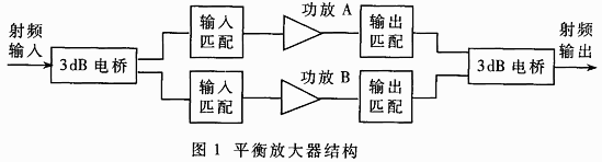
Power amplifier is an important part of digital TV transmitter. Under normal circumstances, the signal in the digital TV transmitter is modulated by the COFDM method to output the intermediate frequency analog signal, which is sent to the amplification part through up conversion. The modulation method includes IFFT (8M) and IFFT (2M) two modes, consisting of 6817 and 1705 carriers respectively. The frequency interval between each carrier is very close, so the intermodulation signal easily falls within the frequency band, causing intermodulation distortion. Digital TV transmitters have higher requirements on linearity and stability than traditional types. The power amplifier in the transmitter is required to work in a higher linear state with stable gain.
Figure 2 Input matching network topology
1 Power amplifier design
Figure 3 Topology diagram of output matching network
The LDMOS manufacturing process combines BPT and gallium arsenide processes. Unlike the standard MOS process, LDMOS does not use the BeO beryllium oxide isolation layer on the device package, but is directly hard-connected to the substrate, the thermal conductivity is improved, the device's high temperature resistance is improved, and the device life is greatly extended . Due to the negative temperature effect of the LDMOS tube, its leakage current is automatically shared when heated, instead of the positive temperature effect of the bipolar tube, which will locally form a hot spot in the collector current, so the tube is not easy to damage. Therefore, the LDMOS tube greatly strengthens the ability to withstand load mismatch and over-excitation. Also due to the automatic current sharing effect of the LDMOS tube, its input-output characteristic curve bends slowly at the 1dB compression point (saturation section used by large signals), so the dynamic range becomes wider, which is beneficial to analog and digital TV RF signal amplification. LDMOS is approximately linear when amplifying small signals, and there is almost no intermodulation distortion, which greatly simplifies the correction circuit. The DC gate current of the MOS device is almost zero, the bias circuit is simple, and no complex active low impedance bias circuit with positive temperature compensation is needed. 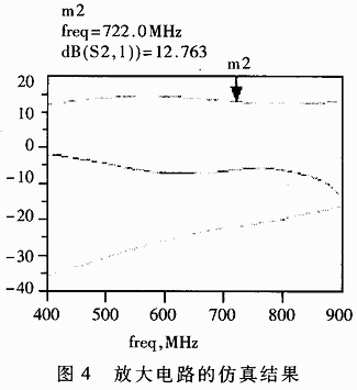
Table 1 Comparison of balanced amplifier and single tube amplifier characteristics Characteristics Balanced amplifier Single tube amplifier Input and output reflection it is good Poor Noise characteristics better Poor Long-term stability it is good Poor Smaller Larger 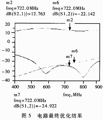
Table 2 SRF parameters of MRF373 under (Vce = 26V Ic = 500mA) 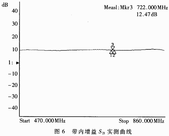
3 Test results
Design of power amplifier in digital TV transmitter
Abstract: Using the latest LDMOS FET device, using a balanced amplifier circuit structure? Smoke power amplifier design in digital TV transmitters. The working frequency band is 470MHz ~ 860MHz, the gain in the whole frequency band is about 12dB, working in the linear state, the intermodulation suppression is less than -35dB.