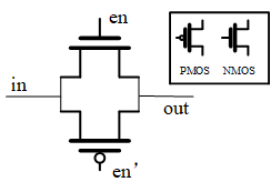
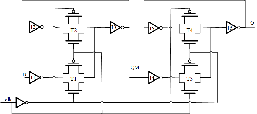
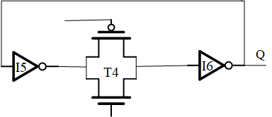
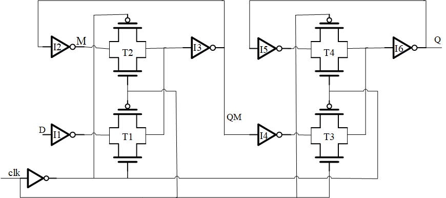
Introduction to registers, setup and hold time, and transmission delay The registered icon is generally as shown in the figure below (ignoring the reset terminal). Let me introduce the transmission gate first. The CMOS transmission gate is shown in the figure below. It consists of a PMOS and an NMOS. En is connected to the G terminal of NMOS, and the reverse of en' is connected to the G terminal of PMOS. We know that when the G terminal of the NMOS is high, both ends of the NMOS tube are turned on; when the G terminal of the PMOS is low, both ends of the PMOS tube are turned on. Therefore, when en is high, both the PMOS and NMOS transistors are turned on, and the input in can be transmitted to the out end; otherwise, the transmission gate is closed. Question: Why use two tubes, one PMOS and one NMOS to realize the transmission gate, instead of just one NMOS tube or PMOS to realize the transmission gate? Answer: I have already mentioned it when I talked about the implementation of the AND OR gate in CMOS. The following shows the MOS-level circuit diagram of the register triggered by the rising edge of the master and the slave. It can be seen that the front and back two circuits are the same, that is, the clk connection of the transmission gate is opposite, so it is called the master-slave type. When the clock signal is low, the transmission gate T1 is turned on, and the data passes through the inverter I1, the transmission gate T1, and the inverter I3 to the QM terminal. At this time, the T2 and T3 transmission gates are closed. T4 is in the conducting state, so the circuit structure of the latter half is as follows at this time. It is equivalent to two inverters connected end to end, which is a trivial memory structure that maintains the data Q unchanged. When the clock clk changes from low level to high level, T3 turns on, and the data originally transmitted to QM when clk is low level is transmitted to the Q terminal behind. T4 is closed at this time. However, the transmission gate T1 is closed after clk becomes high in the first half of the circuit, and new data D cannot enter. At this time, T2 is turned on, and the structure is as follows, which is also a trivial storage structure. At this time, the data sent in when the low level is maintained remains unchanged. From the above analysis, when clk is low, T1 is turned on and the new data is sent to the first stage, but T3 is not turned on and cannot be transmitted to the Q terminal, and T4 is turned on to form a trivial memory structure to maintain The output of Q remains unchanged; when clk changes from low to high, T1 is turned off, and new data will not be transmitted; at the same time, T2 is turned on, forming a latch to keep the data QM unchanged; at the same time, T3 is turned on, QM is transmitted to the Q terminal; T4 is not turned on, and the previously stored data will not affect Q. Therefore, the overall realization is that when the rising edge of clk comes, the data D will be updated to the Q terminal. After the above analysis, let's look at the setup time, hold time, and transmission delay. Setup time (tsetup): That is, the data D needs to be mentioned at least how long it takes to arrive at the rising edge of clk, so that the data collection will not go wrong. It can be seen from the circuit analysis that the data must be sent to the latch of the first stage circuit, that is, the M terminal before the rising edge of the clock arrives. See below. why? Because if the rising edge comes, the data is not sent to the M terminal, when the clock rising edge comes, the signal at the right end of T2 and the M terminal will be inconsistent; the M terminal is the old data, and the right end of T2 is the new data, then the old data may be New data will be washed away. Therefore, when the rising edge of clk arrives, the data needs to pass through I1, T1, I3, and I2 to be transmitted to the M terminal. Therefore, before the rising edge of the clock, tsetup = tI1 + tT1 + tI3 + tI2 time data D must be sent to the input of the register. This time is the delay of three inverters plus a transmission gate. Hold time (thold): After the rising edge of the clock, how long does the data D need to remain unchanged before it will affect the output Q. It can be seen from the circuit that when the clock rising edge comes, T1 is turned off. Even if the turn-off has a delay, the data changes immediately when the rising edge arrives. It still has to pass through an inverter I1 to reach T1, so don’t worry. Data will be sent in, so the hold time can be zero. Of course, this is for this master-slave structure register, and the retention time of other registers is not necessarily zero. Transmission delay (tcq): After the rising edge of the clock, how long does it take for the data to reach the Q terminal. From the circuit analysis, when the rising edge of the clock comes, the data still needs to pass through T3 and I6 to be transmitted to the Q terminal, so the transmission delay of this register is tcq = tI6+tT3. Here just take the master-slave rising edge trigger register as an example to introduce the concept of why registers have setup time, hold time requirements, and transmission delay. For the subsequent static timing analysis using EDA tools, these parameters are directly given by the device or process library. Next, we will continue to discuss the timing issues and timing optimization of the clock synchronization circuit.
White IDC Connector :IDC connector Automotive Connector is a kind of component that electronic engineering and technical personnel often contact. Its function is very simple: in the circuit is blocked or isolated between the circuit, set up a bridge of communication, so that the current flow, so that the circuit to achieve the intended function. The form and structure of automobile connector are changeable. It is mainly composed of four basic structural components: contact, shell (depending on the variety) and insulator. White IDC Connector ShenZhen Antenk Electronics Co,Ltd , https://www.antenkcon.com