8 Inch Tablet
Today let`s talk about 8 inch tablet with android os or windows os. There are many 8 inch tablets on sale you can see at this store. 8 inch Android Tablet is absolutely the No. 1 choice if you are searching a student online learning project. 8 inch windows tablet is more welcome when clients are looking tablet for business application. The most welcome parameters level is 2 32Gb with 4GB lite, 4000mAh, android 11 only around 60usd, price will be much competitive if can take more than 1000pcs. 7 Inch Tablet wifi only, android tablet 10 inch, Amazon 8 inch tablet is also alternative here. Except tablet, Education Laptop, Gaming Laptop, 1650 graphics card laptop, Mini PC and All In One PC are the other important series.
Therefore, you just need to share the configuration, application scenarios, quantity, delivery time, and other special requirements, then will try our best to support you.
Any other thing in China we can do, you can also feel free to contact us.
You will find that cooperating with us is the best choice, not only save time and energy, but also save much cost.
8 Inch Tablet,8 Inch Android Tablet,Amazon 8 Inch Tablet,8 Inch Tablets On Sale,8 Inch Windows Tablet Henan Shuyi Electronics Co., Ltd. , https://www.hnsylabtop.com
Introduction DS2480B is a 1-Wire master (driver) with UART host interface. The device is optimized for power transmission and supports high-speed modes for embedded applications, freeing the host from the task of generating strictly timed 1-Wire waveforms. The DS2480B uses an active circuit to shorten the recovery time at the end of the time slot. Figure 1 shows a simplified circuit diagram of the 1-Wire driver section. 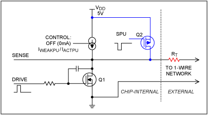
Figure 1. Simplified circuit of the DS2480B 1-Wire driver
When the 1-Wire bus is idle, the DS2480B driver provides pull-up through a controlled current source. The current source can be turned off (during pull-down), can provide weak pull-up current (IWEAKPU during pull-down and idle), or provide an active pull-up (IACTPU at rising edge). The slew rate of the pull-down circuit (Q1) can be adjusted by software. Q2 represents the power supply circuit used by 1-Wire slave functions that require high current (such as EEPROM programming or temperature conversion). The function of Q2 is not discussed in this application note.
To support effective wiring configuration, an external line termination resistance RT (~ 100Ω) is required to minimize the effects of transmission lines, such as reflection, undershoot, and overshoot. However, adding RT will cause the active pull-up to turn off prematurely before the 1-Wire bus is fully charged. This is because the DS2480B detects the voltage on its 1-Wire pin, not the voltage on the slave side of the 1-Wire network. When the voltage on the 1-Wire pin reaches the internal gate limit (typical value IACTPU × RT = 15mA × 100Ω = 1.5V), the voltage on the side of the slave device will be lower than the voltage on the 1-Wire pin, and the difference is the value on RT Pressure drop. The timer starts when the voltage on the 1-Wire pin exceeds this threshold, and the timing must end before the active pull-up is turned off. But since the timer starts early, it ends early. However, after the active pull-up is turned off (initial shutdown), the 1-Wire bus will continue to be charged with the weak pull-up current IWEAKPU until fully charged.
Critical parameters In simple terms, a 1-Wire network can be compared to a lossy capacitor that continuously charges and discharges during communication. Therefore, when determining the performance of the driver, any factors that affect the charging and discharging process of the network are parameters that must be considered. Important parameters describing the hardware definition of the DS2480B driver include: 1-Wire weak pull-up current, IWEAKPU 1-Wire active pull-up current, IACTPU active pull-up threshold, VIAPO active pull-up timer threshold, VIAPYO active pull-up Pulling on time, tAPUOT (2.0µs at standard rate, 0.5µs in high-speed mode) In addition to tAPUOT, the above parameters will change to some extent due to different production batches and different operating temperatures. Because IWEAKPU and IACTPU are affected by the same physical effect, the change trend of the two is the same. In short, if IWEAKPU is greater than the typical value, IACTPU will also be higher than the typical value. Therefore, the ratio of IWEAKPU to IACTPU is almost unchanged. The threshold voltages VIAPO and VIAPYO are independent of each other and are not affected by changes in the pull-up current. For actual parameter values, see the DS2480B data sheet. IWEAKPU is measured when there is a residual voltage of 0.4V on the 1-Wire pin. The DC parameters ΔVSTRPU and ΔVPROG given in the data sheet do not apply to active pull-ups that only occur on the rising edge of the 1-Wire side. In comparison, ΔVSTRPU and ΔVPROG refer to the voltage drop between VDD and 1-Wire or VPP and 1-Wire when a strong pull-up (SPU, powering the slave device) or EPROM programming pulse.
The 1-Wire master timing configuration DS2480B has a scaling rate mode that is different from the standard rate. This special scaling rate mode allows fine-tuning of 1-Wire time slots. The time of the reset / online detection sequence is fixed. The timing parameters that can be set by writing to the control register are as follows: write 1 low time (tLOW1) data sampling offset (tDSO) write 0 recovery time (tREC0) falling edge slew rate (falling edge generated by DS2480B) Table 1 is Selectable ranges and increments of these timing parameters in the scaling rate mode. The parameter value codes and codes are used in conjunction with the DS2480B configuration commands. Table 2 gives the fixed (non-variable) parameters in the telescopic mode and the parameters in the high-speed mode.
Table 1. Variable parameters: only for scaling mode DescripTIon Symbol Par. Code Parameter Value Codes and Values Units 000 001 010 011 100 101 110 111 Write 1 Low TIme tLOW1 100 8 9 10 11 12 13 14 15 µs Data Sample Offset, Write 0 Recovery TIme tDSO, tREC0 101 3 4 5 6 7 8 9 10 µs Pulldown Slew Rate — 001 15 2.2 1.65 1.37 1.1 0.83 0.7 0.55 V / µs
Table 2. Fixed parameters: telescopic mode and high-speed mode DescripTIon Symbol Value (µs) Speed Write 1 High Time tHIGH1 49 Flexible 8 Overdrive Write 0 Low Time tLOW0 57 Flexible 7 Overdrive Active Pullup On-Time tAPUOT 2 Flexible 0.5 Overdrive Write 1 Low Time tLOW1 1 Overdrive Data Sample Offset tDSO 1 Overdrive Write 0 Recovery Time tREC0 3 Overdrive
Data sampling offset and write 0 recovery time parameters are controlled by the same register value. This can be done because both parameters are affected by the charging speed of the 1-Wire network. It is not necessary to sample the 1-Wire (tDSO function) before reaching logic 1. Conversely, the wait time required to fully charge the 1-Wire line during the read time slot can meet the recovery time of the write 0 time slot (tREC0 function).
As shown in Figure 2, the write 1 time slot and read data time slot consist of 3 parts: tLOW1, tDSO and tHIGH1. tLOW1 can be set from 8µs to 15µs. The tDSO range is 3µs to 10µs, tHIGH1 is fixed at 49µs, and the duration of the write 1 or read data slot can be set arbitrarily between 60µs and 74µs. When reading data from the 1-Wire bus (read time slot), sampling is performed within tLOW1 + tDSO time after the start of the time slot, that is, between 11µs and 25µs after the sampling edge starts. 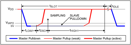
Figure 2. Write 1 time slot and read data time slot
The write 0 time slot (Figure 3) consists of two parts, tLOW0 and tREC0. Since tLOW0 is fixed at 57µs and tREC0 is between 3µs and 10µs, the duration of the write 0 time slot is 60µs to 67µs. According to the data received by the DS2480B from the host UART, there is sufficient idle time between each time slot. 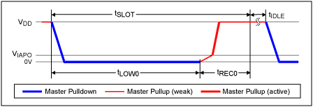
Figure 3. Write 0 time slot
The response time of the 1-Wire slave depends on three factors: the slew rate of the falling edge of the master; the electrical characteristics of the slave; and the physical distance between the master and slave. In the stretch mode, the slew rate can be adjusted with an upper limit of 15V / µs and a lower limit of 0.55V / µs. However, if the slew rate is set lower, conflicts will occur when tLOW1 is set shorter. Multiple tests have shown that 1.37V / µs is an ideal slew rate, suitable for almost all applications with or without line termination. Try to avoid setting to the fastest slew rate (15V / µs) unless the line connection is properly terminated. There may be significant ringing when there is no termination, especially when the DS2480B drives long cables.
How to change the settings is shown in Appendix A, “Choosing Configuration Parameter Valuesâ€. The following configuration is used: tLOW1 = 8µs, tDSO = 9µs, and the best performance is obtained when the timing period is 66µs.
You can download (ZIP) an executable Windows application tmline.exe for setup. The file must be extracted from the ZIP folder and then moved to the Windows desktop. Double-click its icon to run the program, or right-click the icon and select "Open" The program will open a DOS-like window and perform the following tasks: self-test; detect the underlying driver software version; display the default settings of Pulldown Slew Rate, Write 1 Low Time, Data Sample Offset / Write 0 Recovery Time. If the 1-Wire application software is already running when the tmline program starts, the current settings are displayed.
Current (STANDARD) 1-Wire line settings: PDSR = 1.37 V / us W1LT = 8 us DSOW0 = 6 us The first parameter required by the tmline program is Pulldown Slew Rate. The entered value is the parameter value code, as shown in Table A. Enter 0 to 7 to select a new value; enter 8 to exit the program without changing the settings. All other inputs will be ignored.
Select the PDSR (pulldown slew rate): 0) 15 V / us 1) 2.20 V / us 2) 1.65 V / us 3) 1.37 V / us 4) 1.10 V / us 5) 0.83 V / us 6) 0.70 V / us 7) 0.55 V / us 8) EXIT Enter number: 3 (eg user input: 3)
After entering a valid value, the next parameter to be specified is Write 1 Low Time.
Select the W1LT (write-1 low time): 0) 8 us 1) 9 us 2) 10 us 3) 11 us 4) 12 us 5) 13 us 6) 14 us 7) 15 us 8) EXIT Enter number: 0 (Eg user input: 0)
After entering the new Write 1 Low Time, the last parameter entered by the user is Data Sample Offset / Write 0 Recovery Time.
Select the DSO / WOR (data sample offset / write 0 recovery): 0) 3 us 1) 4 us 2) 5 us 3) 6 us 4) 7 us 5) 8 us 6) 9 us 7) 10 us 8) EXIT Enter number: 6 (eg user input: 6)
After entering a valid value, tmline writes a new set of parameters to the DS2480B in the port adapter. It then displays the new setting as the current value in a loop and requests a new falling edge slew rate. Enter "8" to exit the program. While the 1-Wire application software is running, the new settings are always effective.
Multi-slave 1-Wire Network Recovery Time Standard Rate Mode For a single-slave network, under standard speed mode, 1-Wire slave data sheets usually specify a minimum of 2.2kΩ pull-up resistor and a minimum pull-up voltage of 2.8V The recovery time is 5µs. Maxim's application note 3827: Determining the Recovery Time of a Multi-Slave 1-Wire Network describes how to determine the recovery time of a multi-slave 1-Wire network at four different temperatures and two different voltages. Because the DS2480B is a 5V device, you can refer to the application note 3929 for the description of the recovery time when the operating voltage is equal to or greater than 4.5V. When the temperature is higher than or equal to -5 ° C, the recovery time at the standard rate is specified as 2 × N + 1µs (N is the number of slave devices). Therefore, the recovery time of one slave device is 3µs, two slave devices are 5µs, three slave devices are 7µs, and four slave devices are 9µs.
Therefore, according to the worst case (1.5mA IWEAKPU, 9mA IACTPU) calculation in Appendix B, and referring to the configuration of "9 µs recovery time of four slave devices" as a reference, we can know that the DS2480B can handle at least 31 slave devices. Therefore, the driving strength of the DS2480B driver at standard speed is at least 8 times that of the 2.2kΩ active pull-up resistor.
High-speed mode For a single-slave network, in high-speed mode, 1-Wire slave data sheets usually specify a minimum recovery time of 2µs when using a 2.2kΩ pull-up resistor and a minimum pull-up voltage of 2.8V. According to Application Note 3929 mentioned above, when the temperature is higher than or equal to -5 ° C, the recovery time in high-speed mode is 1.37 × N + 0.5µs (N is the number of slave devices). Therefore, the recovery time of one slave device is 1.87µs, two slave devices are 3.24µs, three slave devices are 4.61µs, and four slave devices are 5.98µs.
Therefore, taking the "recovery time of two slave devices as 3.24 µs" as a reference and scaling down to 1.8 slave devices, the recovery time is 3 µs, and then perform the same calculation in the worst case in high-speed mode, you can get The DS2480B can handle at least 9 slave devices. Therefore, the driving strength of the DS2480B driver in high-speed mode is at least 5 times that of the 2.2kΩ active pull-up resistor.
VIAPYO is usually greater than the assumed value in the worst case calculation. As long as the voltage rises sufficiently to be considered the end of the time slot, the slave device allows incomplete recharging. The VIH1 of the DS2480B may be lower than the minimum value specified in the data sheet. However, the reliability of communication will be affected, and the resulting retry will reduce the response speed and throughput.
Summary 1-The reliability of the Wire network depends on both the host (driver) and the slave device. When operating at standard speeds, the DS2480B 1-Wire driver uses the scaling rate and sets tLOW1 = 8µs, tDSO = tREC0 = 9µs to achieve optimal performance. A slew rate of 1.37V / µs is an ideal setting. At this time, the 1-Wire slave device speed range is 15µs to 54µs. When there is only one slave device and the time base is lower than 54µs, the system will not work. The falling edge slew rate becomes 1.65V / µs or 2.2V / µs, which will increase the chance of normal operation of the “critical†slave device in the network. To accommodate slower 1-Wire slave devices (for example, 60µs), tHIGH1 and tLOW0 must be extended by 6µs to 55µs and 63µs, respectively. However, the current version of DS2480B does not yet support this feature.
Take the free Windows software OneWireViewer using a 1-Wire driver as an example. At standard speeds, the OneWireViewer software defaults to tLOW1 = 8µs, tDSO = 6µs, and slew rate of 1.37V / µs. As mentioned above, it will be necessary to increase tDSO to 9µs, and OneWireViewer 4.01 and later will change the default value of tDSO to 9µs to accommodate the recommended values ​​in this application note. The default values ​​of tLOW1 and slew rate are kept at 8µs and 1.37V / µs, respectively.
DS2480B is a strong pull-up 1-Wire driver. Compared with a circuit using a 2.2kΩ pull-up resistor, the driving capability of the DS2480B in standard speed and high-speed mode is at least 8 times and 5 times that of the circuit.
Appendix A. Select the configuration parameter value to write 1 and read data time slot consists of three parts of tLOW1, tDSO and tHIGH1, there are 64 combinations, as shown in Table 3. The longer tDSO (tREC0 when writing time slot 0), the longer it takes for the network to recharge (restore). However, when tLOW1 and tDSO are set to the maximum value, the sampling time will be postponed to 25μs after the start of the time slot. The sampling point is the time when the DS2480B reads the 1-Wire bus.
Table 3. Correspondence between time slot period and tLOW1 and tDSO tLOW1 (µs) tDSO (µs) 3 4 5 6 7 8 9 10 8 60 61 62 63 64 65 66 67 9 61 62 63 64 65 66 67 68 10 62 63 64 65 66 67 68 69 11 63 64 65 66 67 68 69 70 12 64 65 66 67 68 69 70 71 13 65 66 67 68 69 70 71 72 14 66 67 68 69 70 71 72 73 15 67 68 69 70 71 72 73 74
The 1-Wire slave's internal time base varies from 15µs to 60µs. Therefore, when the slave device sends a signal of 0 as a response, it can stop the bus low after 15µs from the start of the time slot. When the slew rate is set to 1.37V / µs (nominal), the slave device responds to the time slot and starts its timer after the voltage reaches approximately 2.2V or tLOW1 for approximately 2µs. To ensure that the signal 0 can still be read in such a fast slave device, the sampling time should not be later than 2 + 15 = 17 µs after the start of the time slot. All timings with a period not exceeding 66µs meet this condition. Another slave device may respond to the time slot and start its timer after the voltage reaches approximately 0.8V or tLOW1 for approximately 3µs, and stop pulling the bus low after 60µs. In this case, the 1-Wire bus can start charging 63 µs after the start of the time slot. In order to set the recovery time to a minimum value of 3µs, the timing period should be a minimum value of 66µs. The fast slew rate can make this time point closer to the time point when the slave device starts the timer. This can slightly improve the recovery time, but if the drive is not connected to the line termination, this also increases the ringing.
What happens if the period of write 1 and read data slot is not 66µs? Fast 1-Wire slave devices support shorter timing periods. However, for every 1µs reduction in the time slot period, the response time of the slowest slave must be 1µs faster. Under the limit of 60µs, the slowest slave device that can work normally in the network cannot be less than 54µs. Slower 1-Wire slave devices allow time slot periods to exceed 66µs. However, for every 1µs increase in the slot period, the fastest slave device must be 1µs slower to maintain its readability in the network. Under the limit of 74µs, the fastest slave device that can work normally in the network cannot be higher than 23µs. The probability that a randomly selected 1-Wire slave device does not meet the last condition above is very low. Therefore, the reliability is poor when the time slot period is less than 64µs or greater than 68µs. Most 1-Wire slave devices have a speed in the range of about 15µs to 60µs, and devices below 54µs are rare.
Since the selected tDSO value is also suitable for recharging tREC0 when writing 0 time slots, tREC0 should be set to the maximum value possible. The maximum value of this value determines better device performance when tLOW1 = 8µs and tDSO = 9µs (highlighted in Table 3). From the perspective of the slave device, the write 0 time slot is analyzed. The slave device starts the timer after about 3µs at tLOW0 and reads the data (sampling) after 60µs. Since the time slot starts after 57µs and tLOW0 ends, the slave starts sampling after 6µs, at which time tREC0 almost ends. In order to ensure that the slave device does not miss the last sampling point of the write 0 time slot, its time base must not be lower than 54µs. This requirement also guarantees that the minimum recovery time for reading a 0 time slot is the same as writing a 0 time slot, which is 9 µs.
Appendix B How many slave devices can the DS2480B drive? This question cannot be answered simply. The 1-Wire slave device is still somewhat different from an ideal capacitor. However, a capacitor model can be used to describe its operation. When the voltage is lower than a fixed value, the capacitor model exhibits a low capacitance value, and when the voltage is greater than this value, the capacitor model exhibits a high capacitance value. The large capacitance value is equivalent to the parasitic power supply capacitance and is used for the recharging process of the slave device.
To speed up the charging process, the DS2480B replaces the resistor with a 2-level current source. At the beginning, charge with a small current IWEAKPU, and then charge with a larger current IACTPU. The rising edge in Figure 4 describes this process in detail. 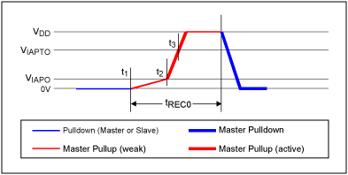
Figure 4. Rising edge
At time t1, the pull-down (master or slave) ends and the weak pull-up current begins to charge the 1-Wire bus. The load on the bus and the IWEAKPU value of the DS2480B determine the rising slope. At time t2, the bus voltage exceeds the threshold voltage VIAPO. At this time, the DS2480B charging current is switched to a relatively large current IACTPU. Therefore, the 1-Wire bus voltage starts to rise rapidly. When the voltage at the time t3 exceeds the threshold VIAPYO, the timer starts to count, so that IACTPU continues to maintain 2µs (tAPUOT, stretch mode) or 0.5µs (high speed mode). After the timer expires, IWEAKPU continues to supply power to the 1-Wire bus until the DS2480B starts the next sequence or communication cycle.
Using a constant current source to charge the capacitor can be described using the following formula:
V (t) = ICHARGE × t / C  (Equation 1)
Set V (t) = VIAPO and make IWEAKPU equal to ICHARGE. The time t2 to reach the threshold VIAPO can be obtained from equation (1) equal to:
t2 = C × VIAPO / IWEAKPU ![]() (Equation 2)
(Equation 2)
At t2, the charging current changes from IWEAKPU to IACTPU, and continuous charging causes the voltage to reach and exceed VIAPYO from VIAPO. Expanding Equation 2 can deduce that the time t3 for charging to VIAPRO is equal to:
t3 = C × [(VIAPTO-VIAPO) / IACTPU + VIAPO / IWEAKPU] ![]() (Equation 3)
(Equation 3)
When estimating the number of slave devices that the DS2480B can drive, it is necessary to divide the recharging process into three stages and analyze each stage separately. Phase 1 Recharge from 0 to 3.6V, the lowest VIAPTO. The end of this phase approximately coincides with the beginning of the slave's recharge. The slave's low capacitance applies. Phase 2 Recharge continues with IACTPU until tAPUOT expires. The slave's high capacitance applies. Phase 3 Recharge continues with IWEAKPU until the next time slot begins. The slave's high capacitance applies.
When estimating the number of slave devices that the DS2480B can drive, it is necessary to divide the recharging process into three stages and analyze each stage separately. The first phase of the charging cycle is calculated using Equation 3. Phase 2 is calculated using Equation 1, let ICHARGE equal IACTPU, and t equal tAPUOT. In this way, the voltage increase caused by the continued charging of IACTPU during the remaining time can be obtained. For the third stage, calculate the remaining charge time and use Equation 1 to determine the extra voltage change caused by IWEAKPU. Given the number of slave devices, if the voltage changes of VIAPYO in the second and third stages cause it to be higher than or equal to the operating voltage, the device is fully charged. The maximum number of slave devices that can satisfy this condition is the desired result. This algorithm can be implemented with a spreadsheet, with the number of slave devices as variables.
After the above calculations, the number of slave devices that can be driven in the stretch mode is 31. Note that this figure is a conservative estimate. The actual number of slave devices that can be driven is more. Table 4 lists the input parameter values ​​used in the calculation.
Table 4. Parameter values ​​used in the calculation of the number of driveable slave devices in the scaling mode Parameter Value Comment Operating voltage 5V Nominal value Slave low capacitance 50pF High estimate, actual value could be lower Slave high capacitance 600pF Typical value VIAPO threshold 1V Typical value Phase 1 threshold 3.6V Lowest VIAPTO specification value Weak pullup current 1.5mA Lowest IWEAKPU specification value Active pullup current 9mA Lowest IACTPU specification value Active current continuation 2µs The continuation timer starts at VIAPTO Recovery time 9µs tRECO
Under the same conditions, high-speed mode can be calculated to drive 9 slave devices. When considering cable capacitance, it must be confirmed that the duration of phase 1 does not exceed 1 µs. Again, this number is a conservative estimate. The actual number of slave devices that can be driven is more. Table 5 lists the parameter values ​​used in the calculation.
Table 5. Parameter values ​​used in the calculation of the number of slave devices that can be driven in high-speed mode Parameter Value Comment Operating voltage 5V Nominal value Slave low capacitance 50pF High estimate, actual value could be lower Slave high capacitance 600pF Typical value VIAPO threshold 1V Typical value Phase 1 threshold 3.6V Lowest VIAPTO specification value Weak pullup current 1.5mA Lowest IWEAKPU specification value Active pullup current 9mA Lowest IACTPU specification value Active current continuation 0.5µs The continuation timer starts at VIAPTO Recovery time 3µs tRECO
Note that for simplicity, it is assumed that the time when the device starts to recharge coincides with the time when the voltage reaches VIAPYO. The actual recharging may start earlier or later, which changes dynamically with the data flow. The earlier the recharging begins, the later it will reach VIAPYO to compensate for the energy required for additional charging. If recharging starts later, less energy is required for charging; the shorter the duration of the first phase, the longer the compensation time for the third phase.
Note that these calculations do not consider the capacitance of the cable connecting the master and slave devices. To find out how many slave devices can be supported with a particular cable, first calculate the cable capacitance and include it in the total capacitance of the slave device when calculating the duration of phase 1 and the voltage changes in phases 2 and 3.
Appendix C Network Overload Conditions The 1-Wire bus has two types of overload, capacitive overload and DC overload. Capacitor overload manifested as insufficient recovery time. It usually appears as a glitch at the end of the write 0 time slot, that is, the next sequence begins when recharging is not completed. If you follow the recommendations in this application note for setup and loading, capacitor overload is unlikely.
If a resistor with a resistance of about 3kΩ is connected between 1-Wire and GND, DC overload will occur. The extra "leakage current" causes the 1-Wire voltage to fall below the driver's supply voltage during the recovery time. If this happens, DC overload will occur on the rising edge, as shown in Figure 5. After the 1-Wire voltage rises to VDD, the 1-Wire voltage will drop to a lower voltage once IACTPU ends. 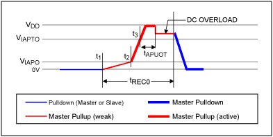
Figure 5. DC overload at rising edge
Understanding and configuration of DS2480B 1-Wire timing
Abstract: The DS2480B is a 1-Wire® host (driver) with a UART host interface. The driver is optimized for power transmission and supports high-speed modes in embedded applications. One of the DS2480B's features is its scalable rate mode, which allows designers to configure 1-Wire timing at standard speeds. This application note explains how to determine the optimal timing configuration and how to use Windows® software to write the setup parameters to the chip. The article also compares the driving strength of the DS2480B and the pull-up resistors. See Application Note 3929 for a detailed description. Appendix I describes how to determine the best configuration parameters. Appendix 2 gives an algorithm for estimating the number of slave devices that the DS2480B can drive, which depends on the electrical characteristics of the host and the capacitive load of the network cable. Appendix III discusses the conditions of network overload.