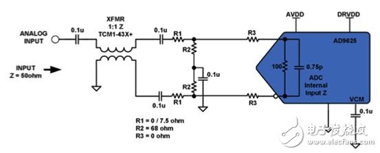
In the ADC, the noise figure (NF) and signal-to-noise ratio (SNR) are interchangeable. The noise figure is useful for understanding the noise density, while the signal-to-noise ratio measures the total amount of noise in the target band. Still, let's take a closer look at the noise figure. Some tradeoffs are misleading, and low noise figures do not always reduce front-end noise in the converter. The noise figure is very convenient to use when trying to understand the dynamic mechanism of the cascaded signal chain. When the source resistance is increased by a factor of 4, the noise figure is increased by 6 dB, but the increased resistance also increases the Johnson noise in the converter. When the source resistance is high or exceeds half of the full-scale input signal on the analog front end (transformer or amplifier), the noise in the target band becomes difficult to control, eventually resulting in reduced converter performance. how so? If you turn down the full-scale input, you must increase the gain. In theory, this does not seem to be a problem, but the dependence of the transformer on the gain bandwidth is higher than that of the amplifier. Therefore, optimizing the noise figure with a high-gain transformer increases the difficulty of implementing common high-IF applications above 100 MHz. A similar problem with amplifiers is that as the gain increases, both signal and amplifier noise increase, which can degrade the performance of the converter. To maintain performance, high-order anti-aliasing filters based on high-loss resistive components are required. When designing the front end of the converter, it is important to consider the noise spectral density (NSD). The noise spectral density, usually in nV/√Hz, is important for converters because the noise spectral density is processed in the digital domain to distinguish and ultimately pick the target signal in the band. Figure 1. Example of the front end design of the AD9625. In summary, the gain is placed in the proper position to ensure that the input and output full-scale signals are maximized throughout the signal chain. In any signal chain, the attenuation, fill bits, or resistance are not benign noise factor tradeoffs because the result is a waste of power and the resistor adds noise. Noise figure = Pf – SNR – 10 log BW + 174 dBm, where Pf is the full-scale power consumption of the input network, SNR is the measured signal-to-noise ratio of the input network, BW is the –3 dB bandwidth of the input network, and 174 dBm is the heat Noise floor; thermal noise floor = kTBW, where k is 1.38 & TImes; 10–23, at room temperature, T is 300K. references Kester, Walt, Analog to Digital, Analog Devices, 2004. ISBN 0-916550-27-3. MT-006: ADC noise figure - a frequently misunderstood technical parameter MT-052: Op amp noise figure: don't be misled Brannon, Brad. Analyze the impact of ADC noise on wireless system performance, EE TImes. 2003 Rob Reeder is a Senior Systems Applications Engineer at Analog Devices, Inc. (Greensboro, NC), and has published numerous papers on converter interfaces, converter testing, and analog signal chain design for a variety of applications. Rob holds a bachelor's and master's degree in electrical engineering from the University of Northern Illinois. Ss Mirror Finished Pedal Dustbin Pedal Bin,Ss Mirror Finished Pedal Dustbin,Ss Foot Pedal Dustbin,Mirror Finished Pedal Dustbin NINGBO ZIXING ELECTRONIC CO.,LTD. , https://www.zixingautobin.com