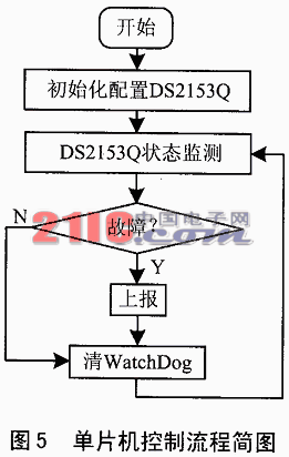
Abstract: HDB3 code has no DC component and has clock recovery and better anti-interference ability. This paper proposes to use HDB3 code for high-speed long-distance data transmission, and gives the NRZ-HDB3 code conversion using the single-chip AT89C51 control E1 transceiver chip DS2153Q, including the circuit design and control software design of the code converter. Keywords: NRZ HDB3 single chip E1 transceiver chip DS2153Q The commonly used NRZ code is not suitable for transmission in the channel of high-speed long-distance data communication, so another code-HDB3 code is selected. HDB3 code is an important coding method for serial data transmission. Compared with the most commonly used NRZ codes, HDB3 has many advantages, such as eliminating the DC component of the NRZ code and having better anti-interference performance for clock recovery, which makes it more suitable for long-distance channel transmission. The E1 signal is HDB3 encoded at a rate of 2.048 Mbps and can be transmitted over 1.5 km on a RJ45 balanced twisted pair with a characteristic impedance of 120 Ω. It can meet the high-speed long-distance transmission of data in most cases. At high speeds with data rates less than 2.048 Mbps, the data rate can be increased by inserting additional data bits. The E1 transceiver chip DS2153Q is fully compliant with the E1 signal standard and has a peripheral microcontroller interface that greatly increases the usability of the chip. E1 has three ways of framing, multiframe and unframed. In the framed E1, the 0th slot is used for transmitting frame synchronization data, and the remaining 31 slots are used for transmitting valid data; in the E1 of the multiframe, except for the 0th slot, the 16th slot is For the transmission of signaling, only the first to fifteenth, a total of 30 slots 17th to 31st can be used to transmit valid data; and in the unframed E1, all 32 slots can be used to transmit valid data. The E1 of the NRZHDB3 code converter proposed in this paper works in unframed mode, that is to say, 32 time slots of E1 are used to transmit valid data. The DS2153Q is a Tallas T1/E1 transceiver chip that complies with the latest E1 line standards, including ITU G.703, G.704, G.706, G.823, I.431, ETSI300 011, 300 233, TBR12, and TBR13. The chip can complete the mutual conversion between NRZ and HDB3 codes, the code rate can reach 2.048Mb/s, and the integrated circuit will recover the circuit when receiving the data of the NRZ code, which is more favorable for the latter stage receiving circuit. On-chip D/A can realize the output waveform of G.703 standard, suitable for twisted pair of 75Ω and 120Ω characteristic impedance, and has perfect data flow status monitoring function, which can indicate the transmission status of data stream in real time. The DS2153Q's peripheral microcontroller interface makes it easy to interface with MCUs such as microcontrollers. Its internal 71 8-bit registers enable the user to configure and monitor the DS2135Q through the MCU. These registers mainly include the receive control register, the transmit control register general control register, the interrupt mask register, and the working status register. Figure 1 shows the internal structure of the DS2135Q. Figure. The NRZ-DB3 code converter is a conversion of NRZ code to HDB3 code and HDB3 code to NRZ code. The design uses dedicated E1 receiver chip DS2153Q and single chip AT89C51 to realize the conversion function of the code system. The code converter converts the input NRZ into an HDB3 code output, and simultaneously receives the data on the E1 line into an HRZ code, and recovers the data clock for use by the subsequent data receiving unit. AT89C51 is an 8-bit single-chip microcomputer of Atmel Company, which is responsible for controlling the working mode and state monitoring of the communication chip DS2153Q, and completing the conversion of NRZ code to HDB3 code and HDB3 code to HRZ code. At the same time, the peripheral circuit of the single chip microcomputer also includes a μP monitoring circuit IMP813L, which is used for improving the anti-interference ability and reliability of the code converter operation. 2 is a block diagram showing the structure of the code converter. The parallel data/address line of the DS2153Q is connected to the P0 port of the MCU; the chip select signal is selected from the P2.0 of the MCU; the read/write signal of the MCU is connected to the read/write signal of the DS2153Q; meanwhile, the two interrupt application lines of the DS2153 and the INT0 of the MCU Connected to INT1. In this way, the DS2153Q can notify the working state of the microcontroller itself in a timely manner by means of an interrupt. The circuit connection diagram of AT89C51 and DS2153Q is shown in Figure 3. Through the above hard connection, the control and status monitoring of the DS2153Q by the MCU are realized. In the circuit design of the DS2153Q, in order to make it work in the unframed mode, the transmitted data is all input from the TSER pin, and the pins TLINK and TSER need to be shorted. The LED is used for the working indication of the converter, which can intuitively judge whether the current data conversion is normal. The code converter uses RJ45 balanced twisted pair with characteristic impedance of 120Ω for data transmission. The DS2153Q transceiver circuit is shown in Figure 4. The input and output turns ratio of the transmission transformer is 1:1.36. 3 MCU control program design The converter microcontroller control program consists of two parts: the function configuration of the DS2153Q and the DS2153Q working status monitoring. The function configuration of the DS2153Q realizes the normal operation of the HDB3 code; the DS2153Q working status monitoring is used to obtain whether the current converter is working properly in real time, and timely report and indicate. 3.1 DS2153Q function configuration After the converter is powered on, the μP monitoring circuit is first effectively reset to ensure the normal initialization of the microcontroller, and a single-chip microcomputer enters the configuration process of the communication chip DS2153Q. 1 Initialize the test register and write 0 to the corresponding test register. 2 The configuration of the Receive Control Register (RCR), including the receive frame mode, automatic resynchronization enable, resynchronization criteria, and receive dynamic storage functions, enables the DS2153Q to receive a single chip to work in the Auto Resync, Disable ElasTIc Store. 3 The configuration of the Transmit Control Register (TCR), including the transmit frame mode, the automatic setting of the fault bit, and the function selection of the 16-bit pin, so that the DS2153Q transmitting unit operates in the E-bits not automaTIcally set in the transmit direcTIon, and according to The current conversion mode has different 16-pin functions, 0=Receive Loss of Sync (RLOS), 1=Loss of Transmit Clock (LOTC). 4 Configure the general control register (CCR) to enable reception and transmission of DS2153Q, HDB3 codes, configuration error counter update time, and prohibit dynamic storage of transmitted data. 5 Initialize the interrupt mask register, enable receiving carrier loss, receive out-of-synchronization interrupt, receive data all 0 and all 1 interrupt, enable transmit clock loss interrupt, through these interrupts, the MCU can know the working state of DS2153Q in time, realize the MCU pair Its implementation monitoring. 7 Initialize the transmission line interface control register, including transmission waveform selection, receive equalizer gain selection, anti-jitter suppressor selection, and so on. The control flow of the MCU is shown in Figure 5. Below is the function configuration program (partial) of the DS2153Q. ;************************************************* ****; MOV A, 02H MOV DPTR, #RCR1 MOVX @DPTR, A ; Write register RCR1 to enable automatic resynchronization NOP MOV A, #04H MOV DPTR, #RCR2 MOVX @DPTR, A ; Write register RCR2, disables elastic storage NOP MOV A, #41H MOV DPTR, #TCR1 MOVX @DPTR, A ; Write register TCR1, TSYNC is the output mode NOP MOV A, #0F9H MOV DPTR, #TCR2 MOVX @DPTR, A ; Write register TCR2, E data bit is disabled automatically set NOP MOV A, #44H MOV DPTR, #CCR1 MOVX @DPTR, A ; write register CCR1, allow receiving and sending NOP; HDB3 code NOV A, #00H MOV DPTR, #CCR2 MOVX @DPTR, A ; write register CCR2, configuration error count register NOP ;************************************************* ******* 3.2 DS2153Q status monitoring design After completing the register configuration of the DS2153Q, the MCU enters the transmission status monitoring program to monitor the normal operation of the DS2153Q in real time, including the reading of the status register and the response of the DS2153Q interrupt, and judge the fault and timely report it. (1) Transmission status monitoring The transmission status monitoring of the DS2153Q is realized by the INT1 of the microcontroller. When the transmit status bit of the status register is set, the DS2153Q generates an interrupt, and the slicer responds to the interrupt to read the fault bit of the current status register. When the reading is completed, it is necessary to write 1 to the status register specific status bit to ensure that the subsequent fault can be correctly set. The status monitor (interrupt 1 handler) for the NRZ transmit clock loss fault is given below. MOV DPTR, #SR2 ; Read DS2153Q Status Register 2 NOP MOVX A, @DPTR ANL A, #04H JNZ ERROR SJMP FAVER ERROR: SETB ERR_SR SJMP LOCKE FAVER: CLR ERR_SR LOCKE: JNB ERR_SR, WORK; judges whether the transmit data clock is lost or not SETB P1.0; fault, work indicator diode off SJMP EVER WORK: CLR P1.0; normal, work indicator diode is bright EVER: MOV DPTR, #SR2 MOV A, #04H MOVX @DPTR,A RETI (2) Receive status monitoring The receive status monitoring of the DS2153Q is implemented by the INT0 of the microcontroller. When the transmit status bit of the status register is set, the DS2153Q generates an interrupt, and the microcontroller responds to the interrupt to read the fault bit of the current status register. When the reading is completed, it is necessary to write a 1 to the specific status bit of the status register to ensure that the subsequent fault can be correctly set. The status monitor program (interrupt 0 handler) for the HDB3 code reception carrier loss fault is given below. MOV DPTR, #SR1 ; Read DS2153Q Status Register 21 NOP MOVX A, @DPTR ANL A, #02H JNZ ERROR SJMP FAVER EPPOR:SETB ERR_SR SJMP LOCKE FAVER: CLR ERR_SR LOCKE: JNB ERR_SR, WORK; judges whether the received carrier is lost or not SETB P1.0; fault, work indicator diode off SJMP EVER WORK: CLR P1.0; normal, work indicator diode is bright EVER: MOV DPTR, #SR1 MOV A, #02H MOVX @DPTR,A RETI 4 Summary NRZ-DB3 code converter uses E1 transceiver chip DS2153Q to complete the conversion of NRZ code to HDB3 code and HDB3 code to NRZ code, realize high-speed long-distance data transmission, and make 2.048Mb/s data stream on RJ45 interface twisted pair The transmission distance of 1.5km is realized, which satisfies most high-speed data transmission. 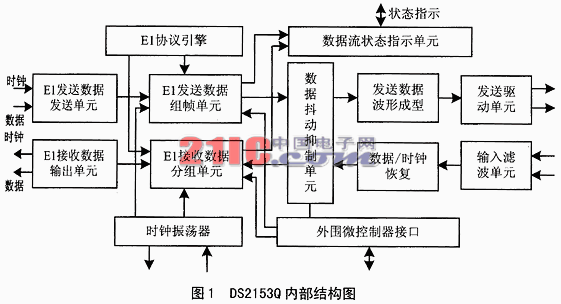
1 E1 transceiver chip DS2153Q brief description 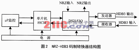
2 code converter circuit design
Figure 3 AT89C51 and DS2153Q circuit connection diagram
The code converter uses IMP813L as the μP monitoring circuit for reliable power-on reset and watchdog control. The clock signal of the DS2153Q is realized by dividing the clock signal of the microcontroller. The single-chip microcomputer selects the clock signal of 16.384MHz, and after using the 74HC74 two-way frequency, the frequency signal of 8.192MHz is obtained as the input clock of DS2153Q. 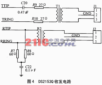
6 Initialize the transmission line interface unit, write 0 to the LIRST data bit, then write 1 to make the transmission line interface enter the normal working mode.