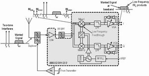
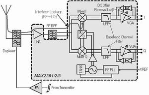
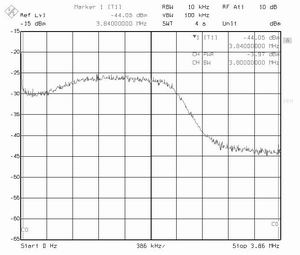
In recent years, with the promotion of 3rd generation (3G) wireless networks in Japan (IMT-2000) , Europe (UMIST) and the United States (CDMA2000) , users of low cost, low power consumption and small form factor required for 3G mobile phones The device (UE) becomes important. The direct down-conversion receiving structure realized by silicon technology and circuit design technology is a promising system solution for 3G mobile phone high integration platform. This paper presents a commercial fully integrated zero-IF receiver solution for 3G radios ( Figure 1) . The receiver input 2nd- order intercept point (IIP2) is widely discussed because it is a key performance indicator for direct conversion receivers. Measurements, simulations, and calculations are given here. Figure 1 Direct Conversion Receiver IC for 3GPP FDD Mobile Radio  Figure 2 : Second- order intermodulation distortion caused by two -tone blocking in a zero-IF receiver  Figure 3 CC reference channel and DL 16 channel blocked CCDF Direct conversion receiver structure As shown in Figure 1 , the direct conversion or zero IF receiver architecture is a way to achieve complete on-chip integration of the receiver, directly demodulating the signals into baseband I and Q signals. In the 3G WCDMA FDD ( full duplex ) mode of operation, only one external duplexer is required to separate the RX and TX sections. Moreover, a post- LAN RF filter is required in FDD radios to suppress out-of-band blocking and transmitter leakage in the demodulator input. In the zero-IF receiver IC , the channel selection of the baseband is achieved by an on-chip low-pass filter. This is followed by channel filtering, where the I/Q signal in the baseband is amplified by a variable gain amplifier (VGA) before being digitized by the analog baseband portion of the radio modem IC . Second order distortion effect In a zero-IF receiver, the second- order intermodulation component (IM2) is an interferer and must minimize these components in the receiver's baseband channel. In the zero-IF receiver, after the front-end second- order nonlinear demodulation of the amplitude modulation signal, the resistance difference component falls into the baseband. Since these second order IM2 component is blocked envelope consisting of a squared term, so the bandwidth of the baseband these undesirable spectral components may reach twice the amplitude of the envelope blocking bandwidth. The IM2 component depends on the desired signal modulation bandwidth in the baseband, so these IM2 components will partially or completely cause receiver interference tolerance. The IM2 distortion component discussed here occurs in a zero-IF receiver downconverter because the low frequency IM2 component in the LNA is typically filtered out by AC coupling or bandpass filtering between the LNA and the mixing unit . There are a variety of IM2 component generation mechanisms in zero IF receivers . However, there are two main sources of IM2 : RF self-mixing: This is due to the non-ideal hard-switching IV characteristics of the conversion stage in the mixer of the zero-IF receiver and the spurious coupling that causes the RF signal to leak into the LO port. Downconverter RF Stage 2nd Order Nonlinearity and LO Level Switching Mismatch: When a strong CW or modulation block is introduced at the I/Q mixer input of a zero IF receiver , the mixer transconductance or RF stage active devices The second order nonlinearity will produce a low frequency IM2 component. IIP2 formula derivation The weak nonlinearity of the receiver front end can be expressed as: ∧          (1) The receiver's input signal ( see Figure 2) is expressed as the total two-tone power equals A2/R . The second- order distortion component of the receiver front end is:      (2) The total output IM2 components ( including the total DC offset ) at (f1+f2) and (f1-f2 ) are expressed as:   (3) The total power associated with the system impedance R in the output IM2 component ( Equation 3) is calculated as follows:            (4) By definition, at the IIP2 power level, the total input signal power is equal to the total power in the output IM2 component ( Equation 4) , divided by the gain factor |a1|2 can be written as:                 (5) According to the total two-tone input power equal to P2T=A2/R , the total power level of the IM2 component associated with the receiver ( Equation 4) can be expressed as:                               (6) IM2 component of the total power level of 4 noted equation, which is a DC of 50% - IM2 component (3dB), the f1-f2 25% (- 6dB ) component, f1 + f2 of 25% (- 6dB ) IM2 component composition. Therefore, the power level of the IM2 component in f1-f2 can be derived from Equation 4 and Equation 6 : (7) Wherein the power level of each tone (f1 or f2 in the P1T) is 50% of the total two-tone power. Effective low frequency IM2 component In 3GPP WCDMA wireless communication, the severe interference to the receiver input is not a two-tone type, but a wideband digital modulation blocking portion. Therefore, it is important to estimate the effective low frequency component of the modulation block to obtain the receiver IIP2 that meets the bit error rate performance requirements . This requires an understanding of the characteristics of the modulation block. In particular, its non-constant envelope is due to its RF blocking to baseband, including the squared term of the envelope. Two major modulation blocks in the 3GPP WCDMA receiver are given in the 3G standard test cases 7.3.1 and 7.6.1 . The first test case, 7.3.1, specifies the minimum sensitivity required for BER < 10-3 when the transmitted uplink (UL) signal is at the maximum power level (+24 dBm) at the antenna . The second test case 7.6.1 specifies the minimum received signal at the antenna connector for BER>10-3 , the modulation downlink (DL) block is -44dBm , 15MHz away from the desired signal , and the UL power is transmitted at the antenna. +20dBm case. The transmission of the UL signal reference measurement channel (12.2 kbps) structure at the antenna of the 3 GW CDMA handset is given in the table of the 3GPP standard document A.1 . It consists of a Dedicated Physical Data Channel (DPDCH) and a Dedicated Physical Control Channel (DPCCH) . In the radio modem section, both the DPDCH and DPCCH channels are extended to 3.84 Mcps , calibrated to the appropriate power ratio (DPCCH/DPDCH = -5.46 dB) , HPSK coded and used with a 1.92 MHz square root cosine (RRC) filter ( roll-off factor a = 0.22) ) Filtering. In addition, the forward channel modulation block ( 15 MHz offset from the desired channel ) consists of the common channel required for testing (Table C.7 calibration ) and 16 dedicated data channels (Table C.6 calibration ) . The signal is QPSK hybrid coded, extended to 3.84 Mcps , coded and filtered with an RRC filter ( similar to a UL signal ) . The signal -3dB bandwidth is equal to 3.84MHz ( in RF) and 99% of the total signal power is within the 4.12MHz bandwidth (-6dBBW) . In order to understand the envelope characteristics of the modulated UL transmit signal or the modulated DL 16 channel signal and to estimate the effective IM2 component of these signals in the WCDMA zero intermediate frequency receiver , the power statistics in each of the signals represented by the complementary distribution function (CCDF) are first investigated . The CCDF gives the peak-to-average power ratio (PAR) of the signal to probability relationship . FIG. 3 shows an ADS (Advanced Design System) simulation CCDF of a UL transmission signal and a DL16 channel signal . Note that in FIG. 3 at 0.1% based on the probability of a transmission of UL DPDCH reference channel, PAR is 3.1dB. In addition, the DL blocking ( at 15 MHz offset ) containing 16 dedicated communication channels has 8.4 dB PAR ( at a probability of 0.1%) , which is almost identical to a Gaussian noise signal. The effective low frequency IM2 component estimation shown below is different from the two standard test cases because the PAR between the two different blocking components is different. Study WCDMA zero-IF receiver input modulated blocker IM2 IM2 component of the ADS simulation template shown in FIG. 4. The IM2 component is filtered by an RRC filter that matches the base station transmitter RRC filter. The total low frequency IM2 component measured in the simulation is within the desired oHz~2.06 MHz baseband signal band, which is half the 99% power bandwidth of the RF signal . The simulated IM2 component spectrum of the WCDMA UL reference measurement channel (12.2 kbps) and WCDMA DL 16 channel blocking at zero intermediate frequency downconverter baseband output is shown in Figures 5 and 6 , respectively . In the ADS template, for simulation, the 0dBm modulation blocking power and the zero-IF downconverter IIP2 equal to +30dBm . For a 0 dBm WCDMA UL transmit signal integrated in the desired signal passband of 1 kHz...2.06 MHz , the total low frequency IM2 component power is equal to -43.7 dBm . DC 2 order nonlinearity caused by offset of 5mV, which is equivalent to generating -33dBm (FIG. 5) of 50 Ω. In addition, for the power level of the total IM2 component of the 0 dBm WCDMA DL 16 channel block , the integral in the desired signal passband of 1 KHz...2.06 MHz is equal to -33.1 dBm . The total DC offset due to the 2nd order nonlinearity is equal to 5mV ( Figure 6) . Equation 6, assuming a zero intermediate frequency converter in accordance with the input of two-tone blocking total power level is zero, the total
Effective IM2 component evaluation for two-tone and WCDMA modulation blocking
introduction