The communication system is inevitably affected by various interferences, so that the information received by the receiving end is inconsistent with the information sent by the transmitting end, that is, the information received by the receiving end generates a bit error. In order to reduce the bit error rate of data communication line transmission, there are usually two methods for improving the quality of data communication line transmission and error detection control. There are many methods for error detection control. This paper discusses the method of parallel implementation of CRC-32 codec in 10G Ethernet access system, and the Unfolding algorithm of parallel CRC algorithm can realize parallel CRC calculation, but the resources used by parallel circuits are increased to the original. J times. The 8-bit parallel CRC algorithm, the parallel CRC-16 encoding logic, and the parallel algorithm given by the parallel CRC algorithm in USB technology are all based on the formula recursion. The recursive algorithm is more applicable when the parallel depth is small. When the parallel depth is large (the 10G Ethernet access system uses a 64-bit parallel data path), the recursive process is too cumbersome and practical. To this end, this paper proposes three algorithms, such as matrix method, substitution method and pipeline method, to solve the implementation problem of CRC algorithm in deep parallel case. Using the algorithm proposed in this paper, the logical expression of 64-bit parallel CRC calculation can be obtained and used in the design of 10G Ethernet access system. Let M/(x) be the information polynomial and G(x) be the generator polynomial. The general CRC encoding method is: first shift the information code polynomial to the left by r, ie, M(x)·xr, and then perform modulo-2 division. (M(x)· xr)/G(x)=Q(x)+R(x)/G(x) (1) The resulting month (x) is the CRC check code. Take the CRC-32 encoding of binary code 0x9595H as an example: · CRC-32G generates multiple G(x)=x32+x26+x23+x22+x16+x12+xll+x10+x8+x7+x5+x4+x2+x+1, converted to hexadecimal code g=0x104C01DB7H. Divide by m by g (modulo 2 division), and the resulting remainder 0x3738F30BH is the CRC-32 code of 0x9595H. The Matlab program that implements the basic CRC-32 encoding of 0x9595H is as follows: g(33:-1:1)=[1,0 0 0 0 0 1 0 0,1 1 0 0 0 0 0 1,0 0 0 1 1 1 0 1,1 0 1 1 0 1 1 1]; a(48:-1:1)=[1 0 0 1 0 1 0 1,1 0 0 1 0 1 0 1,0 0 0 0 0 0 0 0,0 0 0 0 0 0 0 0,0 0 0 0 0 0 0 0,0 0 0 0 0 0 0 0]; For i=48:-1:33, If a(i)= =1 a(i:-1:i-32)=xor(a(i:-1:i-32),i(33:-1:1)); End End Crc=a(32:-1:1) If you want to use the above CRC-32 program to calculate the basic CRC-32 code of other sequences of length L, simply change the upper bound of the array α and the initial value of i in the for loop to 32+L, and use the sequence instead of the array. The starting sequence "1001010110010101" is sufficient. A serial CRC encoder implemented with a digital circuit is shown in FIG. Each rectangle in Figure 1 represents a D flip-flop. The range of gi is 1 or 0. Take 1 to indicate the path, and 0 to indicate the open circuit. When performing basic CRC-32 encoding, each D flip-flop has an initial state of 0, and serially inputs a binary information code from the data side. After the information code is input, the value latched in the D flip-flop is the basic CRC-32 code of the information code. This circuit is suitable for the case where the information code length is an arbitrary value. In some information systems, new rules are added based on the basic CRC generation algorithm. For example, the IEEE802.3 protocol stipulates that the FES (frame check sequence) field of Ethernet is based on CRC-32, and first encodes the first 4 bytes of the information code in the encoding, the destination address, the source address, The length/type field, data field, and PAD field are found after the basic CRC-32 code is obtained, and the result is the FCS. Another implementation equivalent to the above process is to set the initial value of all D flip-flops in Figure 1 so that the result does not have to be negated. In order for the circuit designer to verify that the FCS code is correct, IEEE 802.3 also gives a sample, that is, repeating the sequence 0xBED723476B8FB3145EFB3559H 126 times, and the resulting FCS value should be 0x94D254ACH. 10G Ethernet is a recommendation from the IEEE802.3ae working group. It maintains the frame structure of the previous Ethernet, but the line speed has reached the order of 10Gbps. In order to reduce the power consumption of the 10G Ethernet access system and meet the requirements of the chip processing technology, a parallel data path must be adopted. To calculate the FCS, we need to study the parallel CRC algorithm. The designed 10G Ethernet access system uses a 64-bit parallel data path, so this paper mainly discusses the implementation of 64-bit parallel CRC-32. This paper introduces three implementation methods, in which the matrix method and the substitution method are based on the direct implementation of combinatorial logic, and the third method is based on the pipeline implementation method. The output of the 32 D flip-flops in Figure 1 is d31, d30, ..., d0 from right to left. The input of the information symbol is i. Let D=[d0d1...d31]T denote the current state of the encoder, I=[i63i62...i0] denote the information symbol input of the 1st to 64th clocks, and the vector Dˊ=[d0ˊd1ˊ,...d31ˊ] T denotes The next state of the encoder, D(64), represents the state in which the CRC encoder is after 64 clocks. Then design a 64-bit parallel CRC logic encoder, which is to find the function relationship D (64) = f (D, I). Do'=d31+i63 D1'=d0+d31+i63 D2'=d1+d31+i63 D3'=d2 ... D31'=d30 Written in determinant, with D'=TD+Si63 among them: The state of the encoder after 2 clocks is: D''=TD'+Si62=T)TD+Si63)+Si62=T2D+TSi63+Si62 And so on, there are: D(64)=T64D+T63Si63+T62Si62+...+TSi1+Si0 (2) The semantics of the plus sign in all matrix operations and algebraic operations here are modulo 2 additions. in order to. To design a 64-bit parallel CRC circuit, the large-scale matrix multiplications T64, T63S, etc. in (2) must be calculated. 2 substitution method The advantage of the matrix method is its intuitiveness. But you need to do large-scale multiplication. The substitution method discussed below can achieve the same results as the matrix method. At the same time, large-scale matrix multiplication can be avoided. Let the initial state of the 8-bit parallel CRC-32 circuit be d31, d30, ..., d0, the input is i7, i6, ..., j0, and the output is z31, Z30, ..., z0. Using the matrix method described above, a combined logical expression of an 8-bit parallel CRC-32 encoder can be derived. As shown in Table 1. which is: Z31=d23+d29+i5; Z30=d22+d31+i7+d28+i4 ... Z0=d24+d30+i6+i0 The following uses "+" to indicate the bitwise modulo 2 and the operation, and "{,}" to represent the link operation. The following algorithm is easily derived from the CRC formula (1): Algorithm 1: The CRC-32 of the known sequence N is A[31:0], and the CRC-32 code of the sequence B (=[b7,b6,...,b0]) is Y[31:0]. The CRC-32 of sequence A[31:24] is X[31:0], then the CRC-32 code of the extension sequence {N,B} is {Y[31:24]+X[31:24]+A [23:16], Y[23:16]+X[23:16]+A[15:8]+A[7:0], Y[7:0]+X[7:0]}. Corollary: It is known that the CRC-32 of sequence N is A[31:0], and the CRC-32 of sequence A[31:24] is X[31:0], then the CRC of the complement extension sequence {N,O} The -32 code is {X[31:24]+A[23:16]+A[15:8], X[15:8]+A[7:0], X[7:0]}. The APPEND module is constructed by the above algorithm, and its ports A and B respectively represent the CRC of the preamble sequence and the 8-bit sequence of the extension, and its output port Z is the CRC of the sequence after the extension. Figure 2 constructs a cascaded 64-bit parallel CRC encoder using the APPEND module. This cascaded encoder design is relatively simple. The middle node: Z1(n)=f(r,d[0:7] n[31,0] Z2(n)=f(Z1,d[8:15])=f(f(r,d[0:7]),d{8:15]) ... (3) 3 pipeline method The matrix method and the substitution method are essentially methods for designing direct parallel coding circuits, and the final effect of the two is the same. The CRC encoding circuit control logic implemented directly in parallel is relatively simple, but requires complex combinatorial logic operations. In order to perform parallel CRC encoding at a higher frequency, the coding logic can be further simplified by a pipeline method at the cost of delaying the processing of the entire frame by 8 clock cycles. Figure 4 shows the pipeline implementation of CRC encoding. The 64 bits input in parallel are divided into 7 bytes, which are represented by D0, D1, ..., D7, respectively. The P module (P0~P7) calculates the CRC of a sequence of the form "Di, O, O, O, O, O, O, O, Di", where Diˊ is the last input in the Di position. The CRC code of Diˊ is input by port R[31:0], Di is input by port D[7:0], and the result is output by Z[31:0] port. The inputs of the C modules (C1~C7) are "D0, O, O, O, O, O, O, O, D0' and "D1ˊ, O, O, O, O, O, O, O, D1" CRC (input by ports R1 and R2 respectively), the output is "D0ˊ, D1ˊ, O, O, O, O, O, O, D0, D1" CRC. When the logical expression of P is found, the inference of Algorithm 1 is repeated. , you can find the CRC code of "Diˊ, O, O, O, O, O, O, Di", and then apply Algorithm 1, you can find "Diˊ, O, O, O, O, O, O, O The CRC code of Di". The logic expression of the C module can be obtained by directly applying the algorithm 1. The length of the exclusive OR operation of the P module and the C module is much smaller than that of the ENC8 module in the direct parallel CRC circuit, so it is more advantageous in the high speed circuit. Application. The interface rate required for 10G Ethernet access systems is up to 10Gbps. From the perspective of reducing system power consumption and chip manufacturing cost, it is desirable to operate the interface below 200 MHz. Although the parallelization design can reduce the system clock frequency, it also increases the design difficulty from the following two aspects. First, the more parallel the data path is, the more complex it is to control it. The system uses an 8-byte parallel data path, and the transmitted Ethernet frame may end at any of the 8 parallel bytes. The design of the control logic must consider all of these possibilities and handle them one by one. Second, the design of the CRC encoder, scrambler, etc. in the system must use a parallel algorithm. In order to meet the requirements of the IEEE802.3 protocol for CRC encoding of Ethernet frames, the actual codec module also needs to be able to perform an inverse operation of any number of bytes on the input and output signals. Given the complexity of the 10G access system, the module functionality should be highly integrated to operate with the macro signal port. When verifying the received Ethernet frame, it is not necessary to first calculate the CRC code of the sequence that does not include the FCS domain (the result is inverted) and then compare it with the FCS domain. In the case where the encoding is correct and there is no error, the result of the CRC encoding that does not negate the result of the entire Ethernet frame (including the FCS domain) should be the sequence 0xC704DD7BH. With this discriminating method, it is not necessary to stop calculating the CRC encoding before the end of the frame, and thus the circuit design can be greatly simplified. 5 CRC encoder implementation The hardware implementation of the various algorithms proposed in this paper has been verified by FPGA and applied to specific chips. The CRC encoder and decoder designed by the above-mentioned substitution method and pipeline method were respectively simulated by XC2V1000 in Xilinx's Virtex2 series FPGA, which verified the correctness of the design method. After considering the logic complexity, the occupied chip area and the process requirements, the CRC encoder and decoder designed by the substitution method are finally adopted in the designed 10G Ethernet access chip. A parallel CRC encoder is required in the 10G Ethernet access system. This paper proposes a direct implementation based on combinatorial logic and a pipeline-based implementation. The methods directly implemented are divided into matrix method and substitution method. After specific derivation, it is found that the directly implemented encoder can meet the delay requirement and is therefore adopted by the system. Pipeline-based designs can be used in higher speed applications because of their lower latency. The three parallelization design methods proposed in this paper have passed hardware verification. These design ideas are equally applicable to other linear shift registers, such as the design of scramblers. 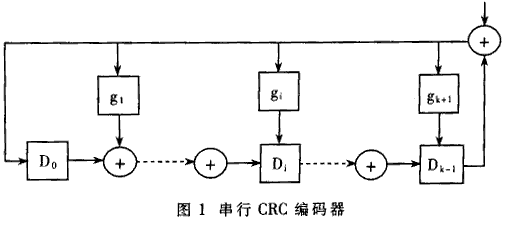
· Change the information code to the left by 32 bits to 0x959500000000H, denoted as m. 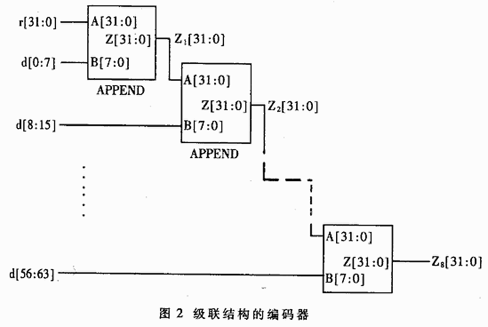
1 matrix method 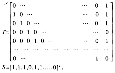
Table 1 8-bit row CRC logic table Z0 D24, d30, i6, i0 Z1 D25, d31, i7, i1, d24, d30, i6, i0 Z2 D26, i2, d25, d31, i7, i1, d24, d30, i6, i0 Z3 D27, i3, d26, i2, d25, d31, i7, i1 Z4 D28, i4, d27, i3, d26, i2, d24, d30, i6, i0 Z5 D29, i5, d28, i4, d27, i3, d25, d31, i7, i1, d24, d30, i6, i0 Z6 D30, i6, d29, i5, d28, i4, d26, i2, d25, d31, i7, i1 Z7 D31, i7, d29, i5, d27, i3, d26, i2, d24, i0 Z8 D0, d28, i4, d27, i3, d25, i1, d24, i0 Z9 D1, d29, i5, d28, i4, d26, i2, d25, i1 Z10 D2, d29, i5, d27, i3, d26, i2, d24, i0 Z11 D3, d28, i4, d27, i3, d25, i1, d24, i0 Z12 D4, d29, i5, d28, i4, d26, i2, d25, i1, d24, d30, i6, i0 Z13 D5, d30, i6, d29, i5, d27, i3, d26, i2, d25, d31, i7, i1 Z14 D6, d31, i7, d30, i6, d28, i4, d27, i3, d26, i2 Z15 D7, d31, i7, d29, i5, d28, i4, d27, i3 Z16 D8, d29, i5, d28, i4, d24, i0 Z17 D9, d30, i6, d29, i5, d25, i1 Z18 D10, d31, i7, d30, i6, d26, i2 Z19 D11, d31, i7, d27, i3 Z20 D12, d28, i4 Z21 D13, d29, i5 Z22 D14, d24, i0 Z23 D15, d25, i1, d24, d30, i6, i0 Z24 D16, d26, i2, d25, d31, i7, i1 Z25 D17, d27, i3, d26, i2 Z26 D18, d28, i4, d27, i3, d24, d30, i6, i0 Z27 D19, d27, i5, d28, i4, d25, d31, i7, i1 Z28 D20, d30, i6, d29, i5, d26, i2 Z29 D21, d31, i7, d30, i6, d27, i3 Z30 D22, d31, i7, d28, i4 Z31 D23, d29, i5 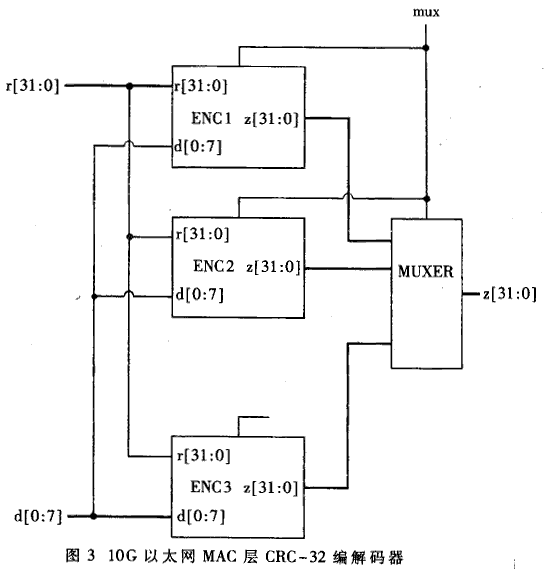
Obviously (3) can be further simplified. Redundant logic makes this cascade structure take up a large chip area and can only be used in low speed applications. For (3) further simplification, the most simplistic or expression of Z2 can be obtained. Similarly, you can get the expression of Z3...Z8. Zl, Z2, ..., Z8 correspond to 8-bit, 16-bit, ..., 64-bit parallel CRC operation expressions, respectively. The specific expressions are limited to the length given here. The longest XOR operation expression in Z8 has 52 entries. If a 4-OR gate is used, only three stages are needed, which can be completed within the first-order transmission delay time of a general CMOS process. When used in an Ethernet access system, because the Ethernet frame does not necessarily end at the 64-bit boundary, the encoder should have the ability to simultaneously compute 8, 16, 24, ..., 64-bit parallel encoding. The specific circuit is shown in Figure 3. Since 64-bit parallel encoding is generally used in a large amount, the usual enable signal mux causes the other 7 encoding modules to be inoperative to reduce power consumption. These 7 modules are used to encode the remaining bytes at the end of the frame. 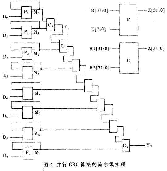
4 CRC codec design in 10G Ethernet access system